Method for anisotropic plasma-chemical dry etching of silicon nitride layers using a gas mixture containing fluorine

a technology of anisotropic plasma and gas mixture, which is applied in the direction of semiconductor/solid-state device manufacturing, basic electric elements, electric apparatus, etc., can solve the problems of significant disadvantage, process, inability to use silicon nitride layers in the reactor chamber, and inability to achieve the effect of alumina-based etching,

Inactive Publication Date: 2003-05-27
ATMEL CORP +1
View PDF22 Cites 230 Cited by
  • Summary
  • Abstract
  • Description
  • Claims
  • Application Information

AI Technical Summary

Benefits of technology

In the event that a noble inert gas, such as argon for example, is used in the inventive method as the non-oxidizing gas, it is possible to achieve an etching selectivity of silicon nitride relative to silicon oxide of greater than 2, already by adding only a small amount of CHF.sub.3 to the SF.sub.6 in the gas mixture. The use of argon relative to helium, for example, achieves the additional advantage that a particularly good uniformity of the silicon nitride etch rate over the silicon nitride wafer surface can be achieved, presumably due to the relatively high atomic weight of argon relative to helium. As a result, it is possible to completely and reliably remove all of the silicon nitride layer using a relatively short over-etching time, for example of only 15% or less, or preferably even less than 10% (e.g. 9 or 9.5%) of the total etching time.

Problems solved by technology

While the patent points out that the etching selectivity of the silicon nitride relative to the resist and of the silicon oxide relative to the resist, respectively, is improved by using the gas mixture of SF.sub.6 and CHF.sub.3, a significant disadvantage is also apparent from the data shown in Table 3.
While that may not be significant in the context of the patent, wherein a silicon nitride layer and a silicon oxide layer are both to be etched selectively relative to a resist layer and a metal underlayer, it is a disadvantage in any application in which a silicon nitride layer is to be etched selectively relative to a silicon oxide layer.
In all dry etching processes using O.sub.2 as a component of the etching gas mixture, there arises the substantial disadvantage that such processes, i.e. such gas mixtures, cannot be used in the reactor chambers of dry etching systems that use oxidizing or oxidizable electrode materials such as silicon or carbon, because such electrode materials would be attacked and corroded due to the effects of the oxygen component of the gas.
Since these gases, or gas components, are corrosive and toxic, they are not suitable for use in all reactors.
Due to the corrosiveness and toxicity of the gas or its components, such an etching gas is also not suitable or acceptable in all applications.
This leads to very low etching rates, which are not practically applicable for etching relatively thick layers, or any layer other than the very thinnest layers.
In the context of the above discussed conventional etching processes, and in addition to the above mentioned disadvantages of the prior art when using oxygen and halides especially containing Cl.sub.2 and Br, studies and experiments conducted by the present inventors have shown that all previously known processes are unable to achieve an adequate or satisfactory control of the edge slope angle of the etched edge of the silicon nitride material.
Namely, the resulting slope angle of an edge of an opening or etched-away area of the silicon nitride layer, which is exposed by a corresponding opening in a resist layer or mask, is variable and not readily controllable using the prior art processes.
Thus, if the layer thickness of the Si.sub.3 N.sub.4 material to be etched is greater than 150 nm, or if the edge slope angle serves an important function for the semiconductor component being fabricated, then the prior art processes are not adequate for achieving the required degree of control of the etched edge slope angle.

Method used


Image

  • Method for anisotropic plasma-chemical dry etching of silicon nitride layers using a gas mixture containing fluorine
  • Method for anisotropic plasma-chemical dry etching of silicon nitride layers using a gas mixture containing fluorine
  • Method for anisotropic plasma-chemical dry etching of silicon nitride layers using a gas mixture containing fluorine

Examples


Embodiment Construction

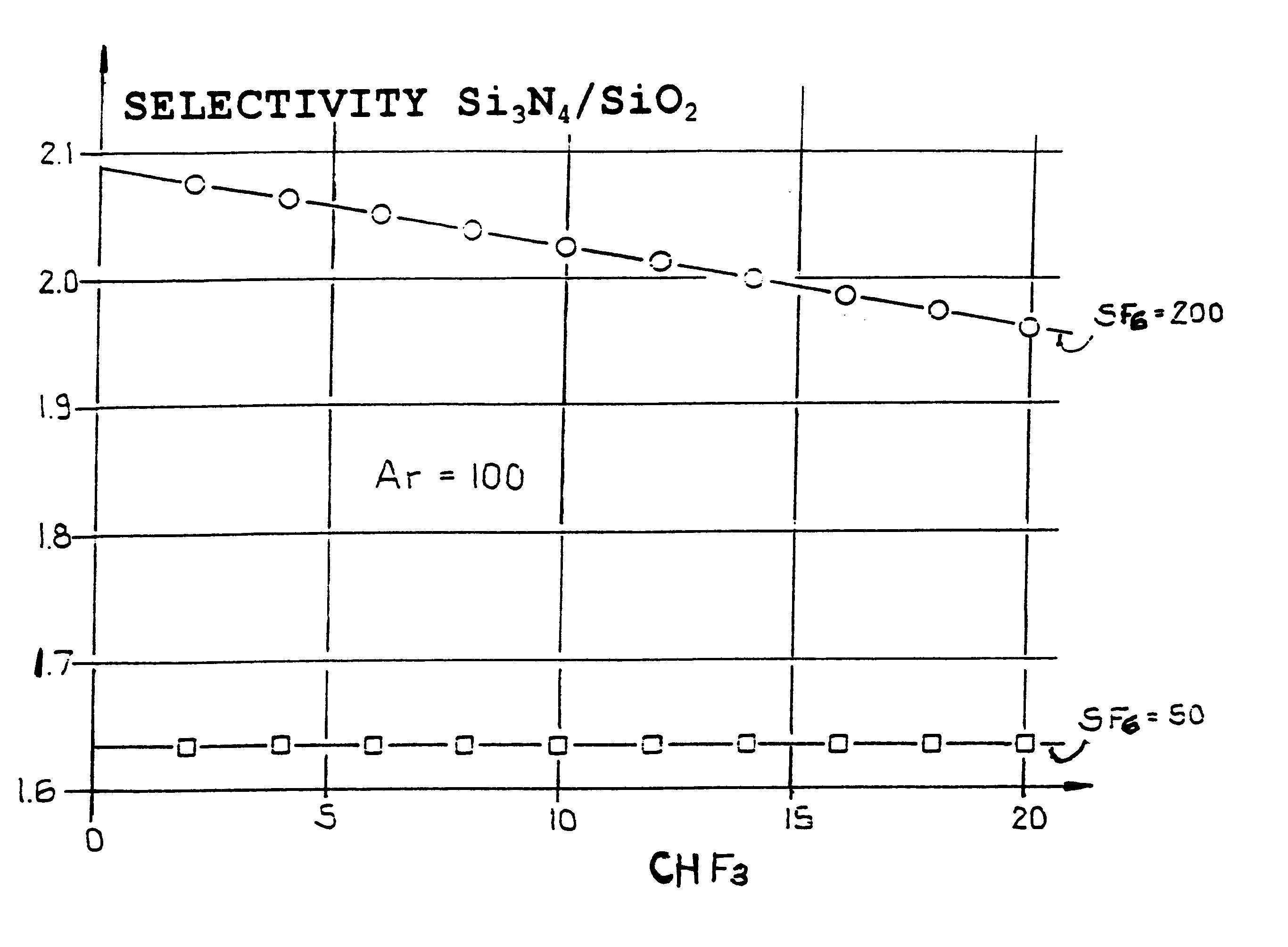
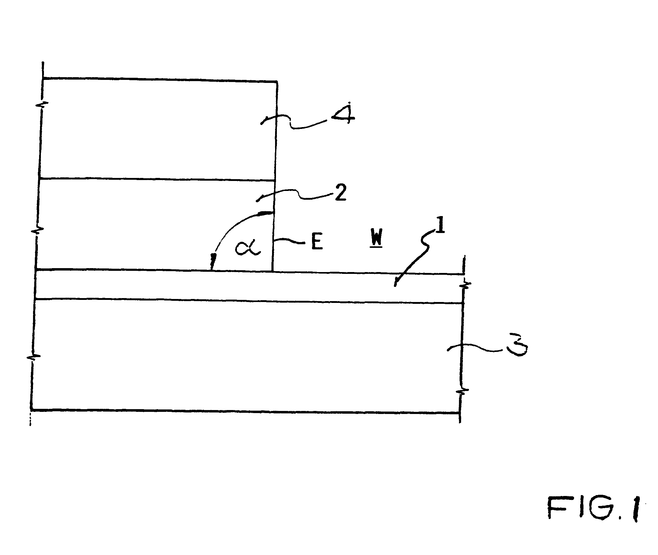
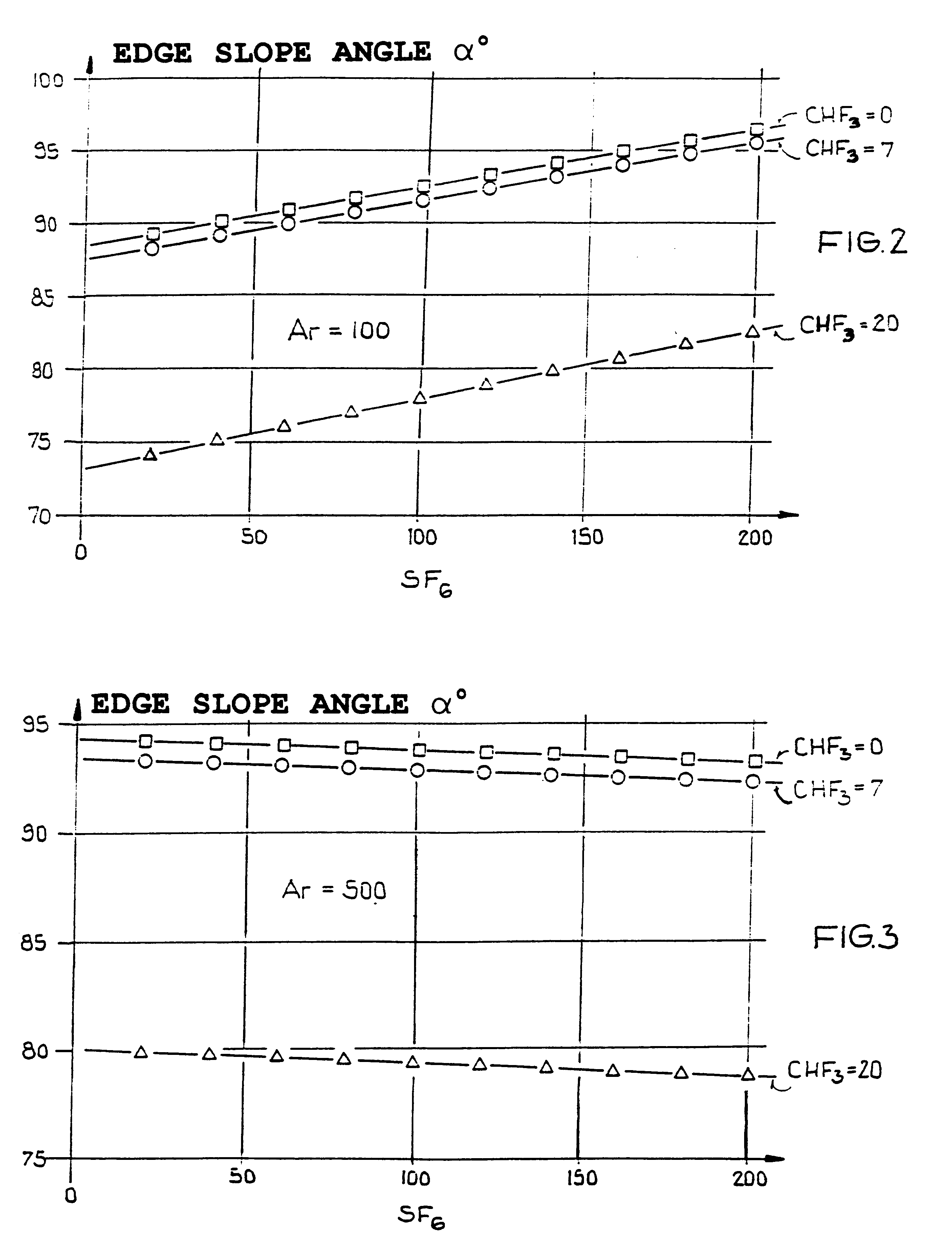
FIG. 1 schematically shows a side view or a cross-section of a layered semiconductor structure that has already been etched by an etching process according to the invention, to form a window or opening W bounded by an etched edge E, as will be described in detail below. The illustrated semiconductor structure was formed by a process as follows.

In a first step, a first or lower semiconductor layer 1 comprising or preferably essentially consisting of SiO.sub.2 was applied on a substrate material 3, for example comprising or essentially consisting of silicon. In the case of using silicon as the substrate material 3, the semiconductor layer 1 of SiO.sub.2 can be formed thereon either by thermal oxidation of the silicon of the substrate 3, or by deposition of a silicon oxide layer by a CVD or a PECVD process. The manner in which the various layers in the presently described structure are formed is not a significant feature or limitation of the invention, and can be carried out according ...


PUM


Abstract

An etching gas mixture containing CHF3, SF6 and a non-oxidizing gas such as Ar is used as an etching gas mixture for the anisotropic plasma-chemical dry-etching of a silicon nitride layer differentially or selectively relative to a silicon oxide layer. The gas mixture does not contain oxygen, chlorine, bromine, iodine or halides in addition to the above mentioned constituents, so that the process can be carried out in reactor systems equipped with oxidizable electrodes. By adjusting the gas flow rates or composition ratios of CHF3, SF6, and argon in the etching gas mixture, it is possible to adjust the resulting etching selectivity of silicon nitride relative to silicon oxide, and the particular edge slope angle of the etched edge of the remaining silicon nitride layer. A high etch rate for the silicon nitride is simultaneously achieved.

Description

PRIORITY CLAIMThis application is based on and claims the priorities under 35 U.S.C. .sctn.119 of German Patent Application 198 60 271.5, filed on Dec. 24, 1998, and German Patent Application 199 55 145.6, filed on Nov. 17, 1999, the entire disclosures of which are incorporated herein by reference.The invention relates to a method for carrying out anisotropic plasma-chemical dry etching of silicon nitride layers using an etching gas mixture particularly containing SF.sub.6 and CHF.sub.3.BACKGROUND INFORMATIONVarious techniques of plasma-chemical dry etching, such as reactive ion etching (RIE) for example, are well known and are typically used in the fabrication of semiconductor circuit elements. An advantage of such dry etching techniques in comparison to wet etching techniques is that structures having dimensions of less than 1 .mu.m can be produced using dry etching but not by using wet etching. This is necessary, for example, for fabricating integrated circuit elements with SiGe ...

Claims


Application Information

Patent Timeline
Patent Type & Authority Patents(United States)
IPC IPC(8): H01L21/02H01L21/311
CPCH01L21/31116
Inventor GELLRICH, NORBERTKIRCHMANN, RAINER
Owner ATMEL CORP
Why Eureka
Try Eureka