

Method of forming fine pattern
- Summary
- Abstract
- Description
- Claims
- Application Information
AI Technical Summary
Problems solved by technology
Method used
Image

Examples
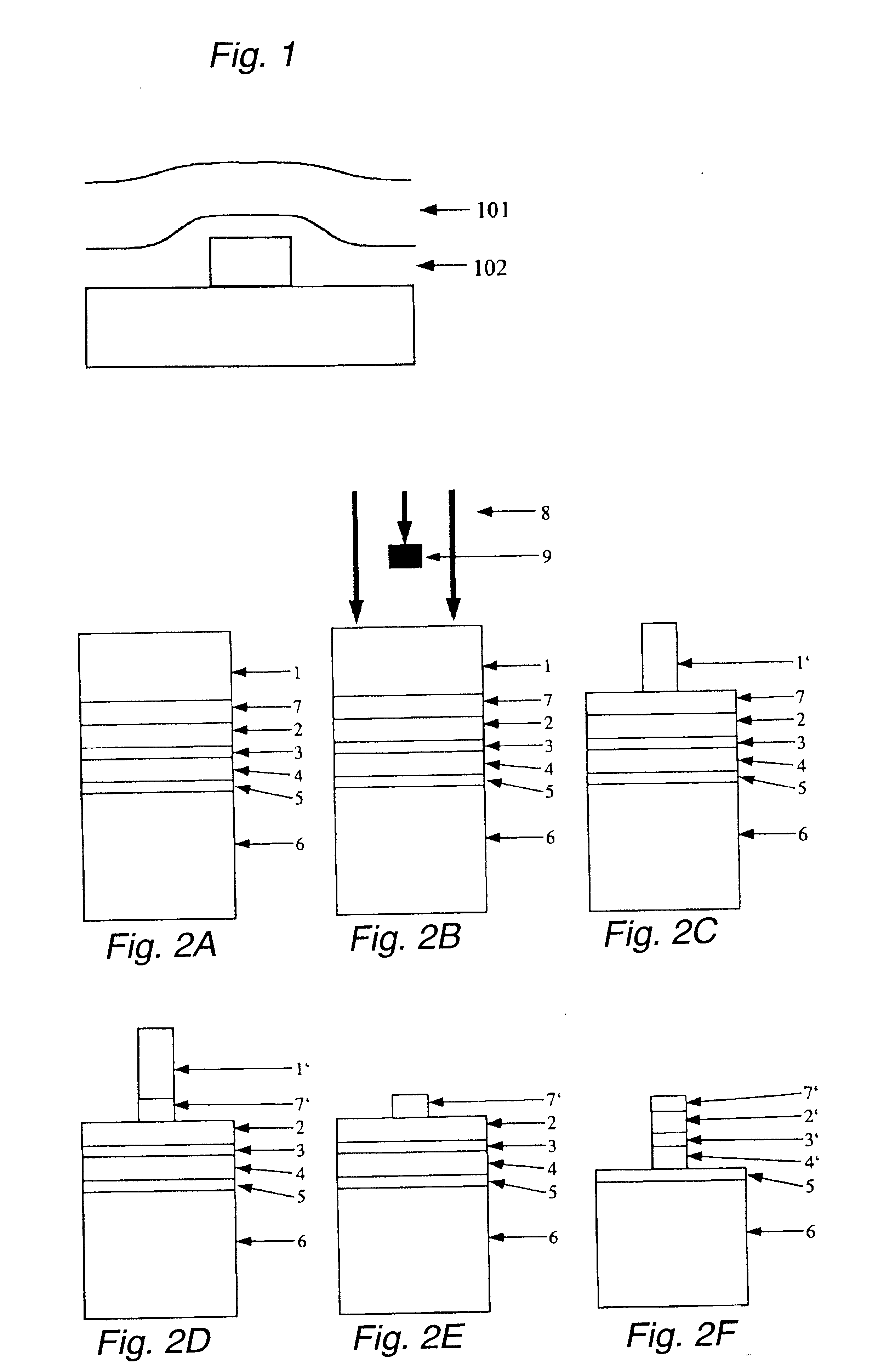
first embodiment
In the first embodiment, the wavelength of exposing radiation used for irradiating the photoresist 1 is limited to a value of 193 nm. However, the present invention is not limited to such a value and can yield the same advantage in the case where exposing radiation assumes a wavelength of 195 nm or less.
In the first embodiment, the refractive index of the silicon nitride film 7 is limited to a value of 1.959, and the extinction coefficient of the same is limited to a value of 0.448. However, the present invention is not limited to these values. More specifically, so long as the refractive index of the silicon nitride film 7 falls within the range of 1.4 to 3.5 and the extinction coefficient of the same falls within the range of 0.2 to 0.8, there can be yielded the same advantage as that yielded by the first embodiment.
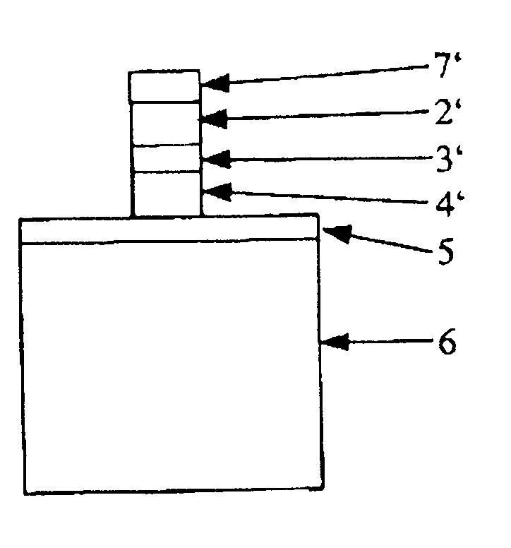
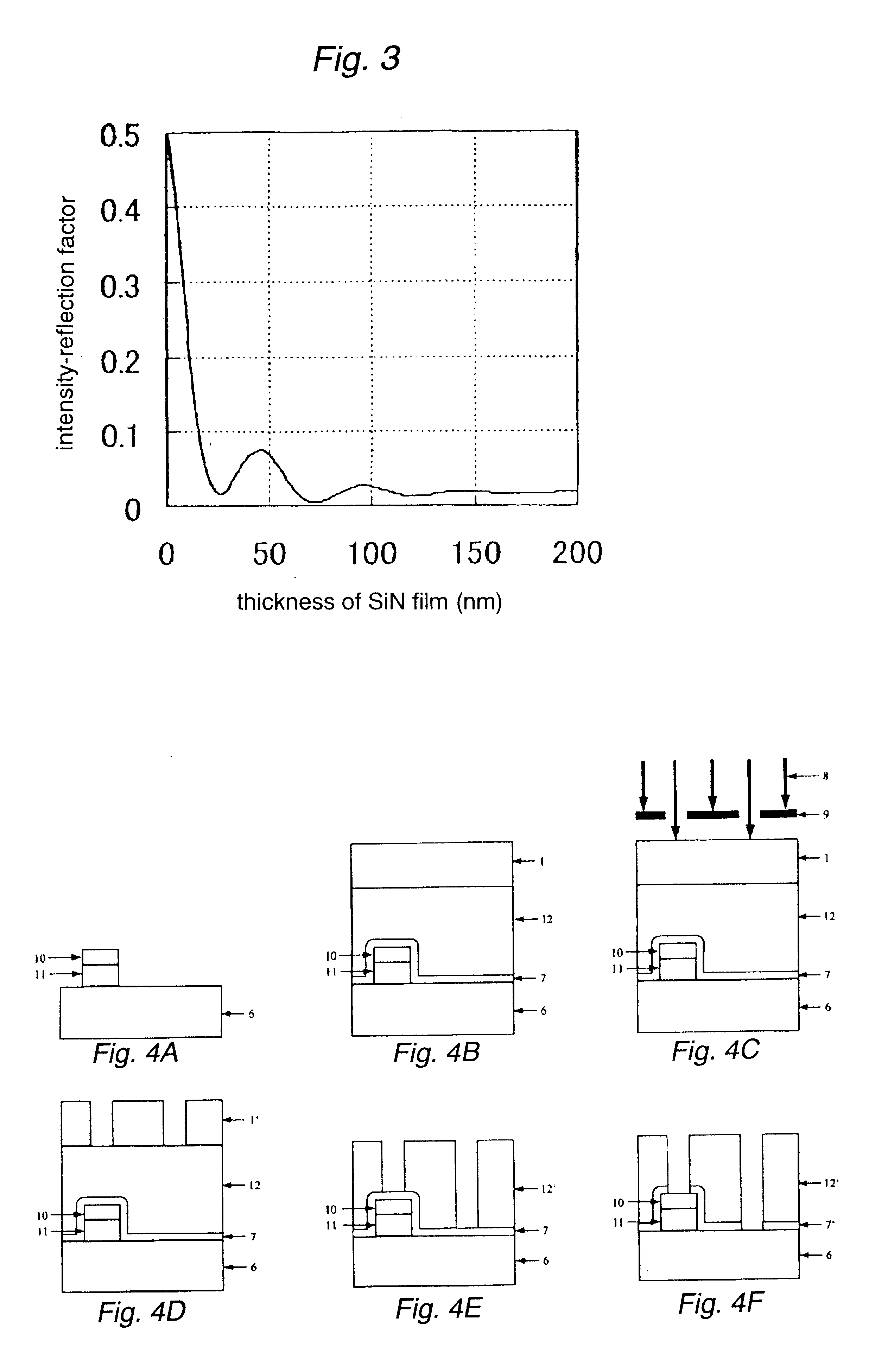
In the first embodiment, the thickness of the silicon nitride film 7 is limited to a value of 73 nm. However, the thickness is not limited to such a value and assumes ...
second embodiment
A second embodiment of the present invention will now be described by reference to FIGS. 4A through 6B.
FIGS. 4A through 4F are illustrations for describing steps of a fine pattern formation method according to the second embodiment. In FIGS. 4A through 4F, those elements which are identical with or correspond to those shown in FIGS. 2A through 2F are assigned the same reference numerals, and repetition of their explanations is omitted here.
In FIGS. 4A through 4F, reference numeral 10 designates a processed tungsten silicide film (WSi film); 11 designates a processed amorphous silicon film; 12 designates a BPSG film before processing; and 12' designates a BPSG film after processing. An oxide silicon film (not shown) is interposed between the amorphous silicon film 11 and the substrate 6, to thereby isolate the film and substrate from each other.
As shown in FIGS. 4A through 4F, according to the fine pattern formation method of the second embodiment, the silicon nitride film 7 is depos...
third embodiment
A third embodiment of the present invention will now be described by reference to FIGS. 7A through 10B.
FIGS. 7A through 7F are illustrations for describing steps of a fine pattern formation method according to the third embodiment. In FIGS. 7A through 7F, those elements which are identical with or correspond to those shown in FIGS. 2A through 2F or FIGS. 4A through 4F are assigned the same reference numerals, and repetition of their explanations is omitted here.
In FIGS. 7A through 7F, reference numeral 13 designates a polycrystalline silicon film before processing; 13' designates a processed polycrystalline silicon film after processing; 14 designates a silicon oxide film before processing; and 14' designates a silicon oxide film after processing. An oxide silicon film 5 is interposed between the polycrystalline silicon film 13 or 13' and the substrate 6, to thereby isolate the film 13 from the substrate 6.
As shown in FIGS. 7A through 7F, according to the fine pattern formation meth...
PUM
| Property | Measurement | Unit |
|---|---|---|
| Temperature | aaaaa | aaaaa |
| Angle | aaaaa | aaaaa |
| Substance count | aaaaa | aaaaa |
Abstract
Description
Claims
Application Information