Zirconium-doped BST materials and MOCVD process forming same

a technology of zirconium-doped bst and mocvd, which is applied in the direction of oxide conductors, conductors, non-metal conductors, etc., can solve the problems of strong short-circuit current, catastrophic failure of dielectric devices made from these materials, and relatively low breakdown strength of conventional ferroelectric materials

Inactive Publication Date: 2003-07-29
ENTEGRIS INC
View PDF4 Cites 35 Cited by
  • Summary
  • Abstract
  • Description
  • Claims
  • Application Information

AI Technical Summary

Problems solved by technology

Despite their advantages and favorable characteristics, these conventional ferroelectric materials have an associated disadvantage of relatively low breakdown strength.
As a result, dielectric devices made from these materials can fail catastrophically when applied voltage rises above a specific level and causes strong short-circuit currents.
Since energy storage capacity of a capacitor positively correlates with the square of applied voltage on such capacitor, limitations on applied voltage correspondingly limit the electrical energy storage characteristics of the capacitor.
Further, conventional ferroelectric materials exhibit high current leakage under elevated voltage conditions.
This in turn leads to high power dissipation as evidenced by high loss tangent .delta. of the material.
The high power dissipation rate greatly reduces the energy storage efficiency of corresponding dielectric devices fabricated from such conventional ferroelectric materials.
Unfortunately, the permittivity of these materials is very low, usually in the range from 3 to 20.
Such low permittivity results in unsatisfactorily low specific capacitance of these dielectric materials, rendering them unsuitable for energy storage applications in integrated circuit devices.
Growth temperature of a perovskite crystal material thin film deposited by MOCVD process has a significant impact upon crystalline structure of the thin film that is deposited, which consequently affects dielectric properties of such thin film.
Conventional undoped BST material has high tunability, which means that its dielectric constant shifts with applied voltage or frequency and therefore becomes "tunable" under changing voltage or frequency conditions.
However, the conventional BST material, due to its large loss tangents, tends to dissipate electronic energy at a high rate with consequent high energy wastage.
Additionally, the loss tangent of the conventional BST material significantly increases at low and high frequencies.

Method used


Image

  • Zirconium-doped BST materials and MOCVD process forming same
  • Zirconium-doped BST materials and MOCVD process forming same
  • Zirconium-doped BST materials and MOCVD process forming same

Examples


Embodiment Construction

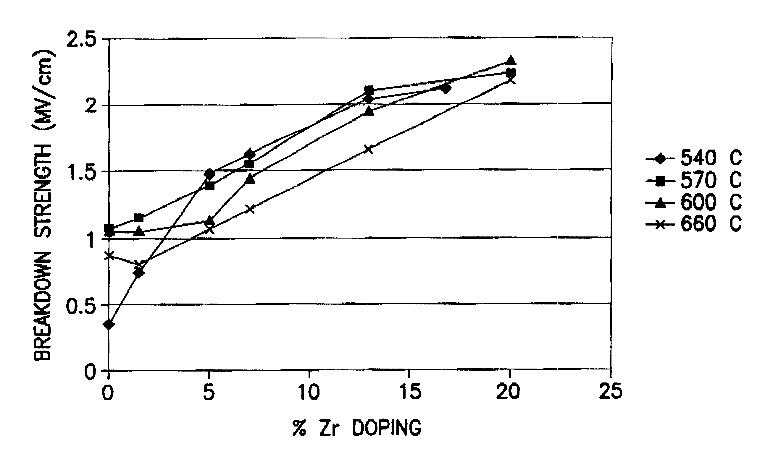
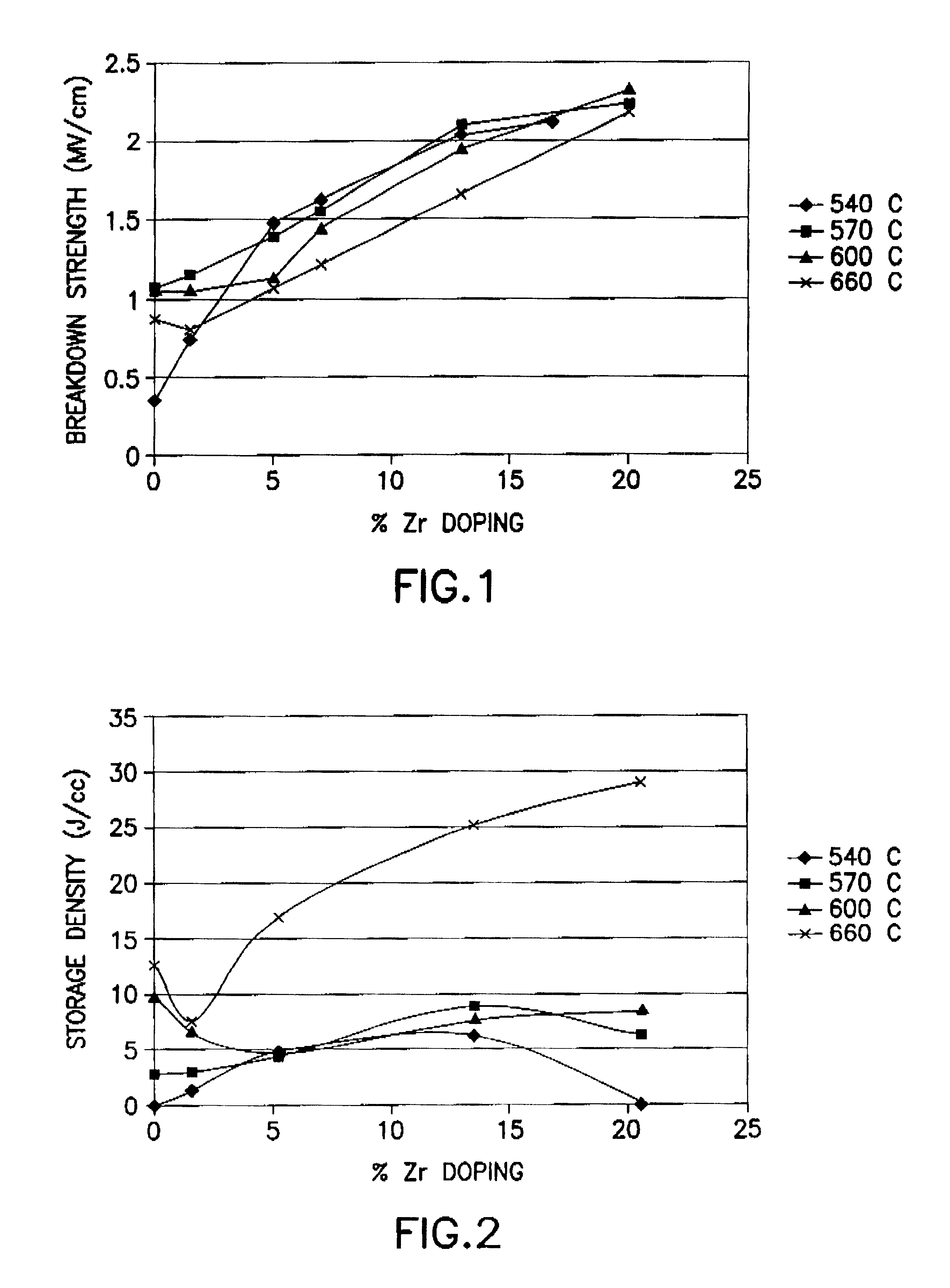
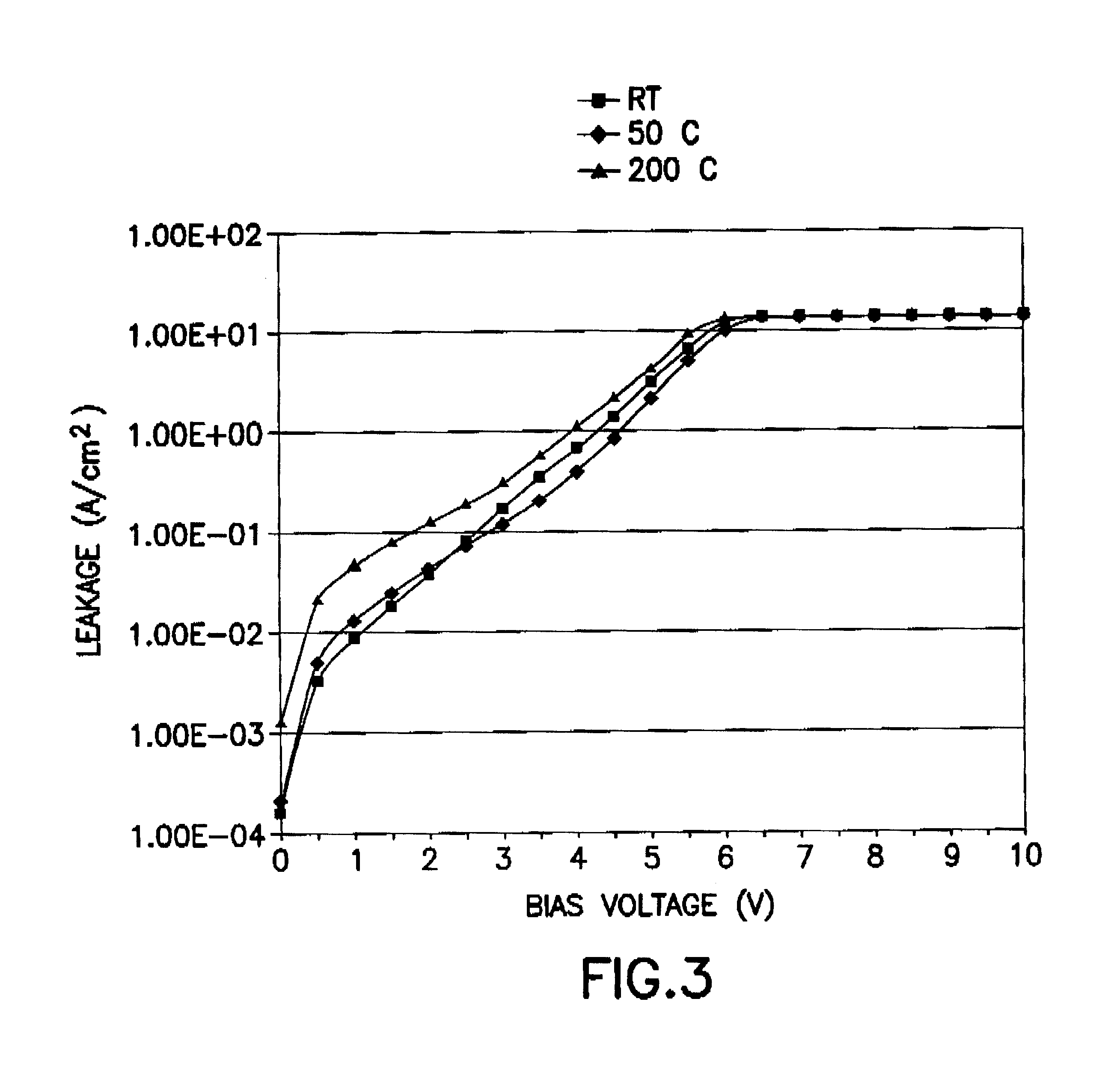
The present invention provides improved BST perovskite crystal thin films suitable for manufacturing high performance microelectronic devices, as well as a commercially useful process for forming such thin films.

In bulk BST ceramic materials, the addition of zirconia significantly reduces loss tangent of the mixture of BST and zirconia. Sengupta et al. U.S. Pat. No. 5,486,491 (hereinafter "Sengupta") discloses a ceramic ferroelectric material with the general compositional formula (Ba,Sr)TiO.sub.3 --ZrO.sub.2, prepared by obtaining powders of BST and zirconia, mixing such powders in a desired weight percentage, ball milling such mixture in an organic solvent with a binder, air-drying such mixture, dry-pressing and sintering the final mixture under high pressure and elevated temperature to obtain a bulk BST-zirconia ceramic (see Sengupta, column 4, lines 6-24). However, such bulk BST-zirconia ceramic contains BST and zirconia only as mixed microparticles, not as a single compound. Zi...


PUM

PropertyMeasurementUnit
energy storage densityaaaaaaaaaa
thicknessaaaaaaaaaa
thicknessaaaaaaaaaa

Abstract

A Zr-doped (Ba,Sr)TiO3 perovskite crystal material dielectric thin film. Such dielectric thin film is characterized by at least one of the characteristics including: (a) a breakdown strength of at least 1.3 MV / cm; (b) a leakage current of not more than 1x10⁻³ A / cm2 under applied voltage of about ±3V or above and at temperature of about 100° C. or above; and (c) an energy storage density of at least 15 J / cc. The dielectric thin film comprises zirconium dopant in the amount of 0.5% to 50% by total weight of the Zr-doped (Ba,Sr)TiO3 perovskite crystal material, preferably 2-15%, more preferably 4% to 14%, and most preferably 5% to 12%. Such dielectric thin film in a preferred aspect is deposited by a MOCVD process using metal precursors Ba(thd)2-polyamine, Sr(thd)2-polyamine, Zr(thd)4, and Ti(OiPr)2(thd)2 at a deposition temperature in the range from about 560° C. to 700° C.

Description

1. Field of the InventionThe present invention relates to metalorganic chemical vapor deposition (MOCVD) formation of (Ba,Sr)(Zr,Ti)O.sub.3 perovskite crystal thin films of high breakdown strength, low leakage, low loss tangent, high permittivity, and substantial tunability with application of electric fields. Such (Ba,Sr)(Zr,Ti)O.sub.3 thin films can be used to manufacture dielectric capacitors or other related microelectronic devices of significantly improved performance useful in many applications, especially for use under elevated temperature and / or high frequency.2. Description of the Related ArtA wide variety of semiconductor materials is used in integrated circuitry for electronic devices. Increasingly more compact integrated circuits with greater capacities are required for new devices, as well as existing device applications. This in turn necessitates the use of materials with higher specific capacitance in order to further reduce the size of individual transistors and capa...

Claims


Application Information

Patent Timeline
Patent Type & Authority Patents(United States)
IPC IPC(8): C23C16/40H01L21/02H01L21/316H01L21/314
CPCC23C16/409H01L21/31691H01L21/02197H01L21/02205H01L21/02271
Inventor STAUF, GREGORY T.CHEN, PHILIP S.ROEDER, JEFFREY F.
Owner ENTEGRIS INC
Why Eureka
Try Eureka