Real-time decoder for scan test patterns

a real-time decoder and scan test technology, applied in the field of real-time decoder for scan test patterns, can solve the problems of limiting the maximum number of scan chains and the shift cycle rate, requiring more than one complete load, and longer scan chains, so as to achieve cost-effective integration

Inactive Publication Date: 2003-08-26
GOOGLE LLC
View PDF3 Cites 84 Cited by
  • Summary
  • Abstract
  • Description
  • Claims
  • Application Information

AI Technical Summary

Benefits of technology

Thus, it is an object of the invention to provide a low-cost test pattern decoding means that can be cost-efficiently integrated into each IC under test.
It is still another object of the invention to establish a simple test pattern encoding scheme that permits preparing test data in a properly encoded form that is compatible with the decoding means provided by the decoding network.
It is a further object of the invention to overcome the above stated limits of previous methodologies by allowing the ATE to continuously supply independent variable data while the internal scan chains are shifted.
The proposed novel decoder circuitry consists of a particularly simple and small logic network that connects the narrow scan data interface of the ATE to a much larger number of internal scan chains inside the IC under test. For example, a decoder network with an amplification factor of 8 expands the 32-bit encoded data words from the ATE into 256-bit wide decoded data words that are shifted into 256 internal scan chains in parallel. The amount of encoded data supplied by the ATE to completely load the scan chains consequently is much smaller (e.g., up to a factor of 8) than the total number of register elements in the scan chains. Because the number of scan chains inside the IC can be made so much larger than the width of the ATE's scan interface, it is possible to proportionally reduce the length of the longest scan chain. The net result is a commensurate reduction of test time (e.g., up to a factor of 8).
For the complete methodology, an equally simple encoding algorithm allows Automatic Test Pattern Generation (ATPG) software to organize the test data in appropriately encoded form for use with the proposed decoder hardware. The key contributing characteristic of automatically generated scan tests is that only a very small subset of register element data values needs to be at a specific "care" value for any given test, while the vast majority of data values are "don't cares". The proposed encoding algorithm exploits both, the sparseness of the "care" values and the freedom to arbitrarily assign "don't care" values, to achieve a significant reduction in the encoded data without losing test coverage.
Despite being simple and requiring a uniquely small circuit overhead in the ICs under test, the disclosed method achieves a large reduction in ATE-resident test data volume and test time when compared to current practices of traditional scan test methods. Because the proposed decoding is performed on the IC under test, no special ATE hardware or software features are needed. The disclosed invention, thus, extends the useful lifetime, and vastly improves the productivity of lower-cost and existing ATE equipment. Since the ATE consumes a considerable portion of semiconductor manufacturing capital investment and operating costs, the invention has the potential of measurably improving the profitability of manufacturing semiconductor products.

Problems solved by technology

Furthermore, some scan tests may require more than one complete load to achieve fault detection.
Furthermore, typical ATEs often limit the maximum number of scan chains and the shift cycle rate.
The fixed width and bandwidth of the scan interface result in longer scan chains and increased test time as the complexity of ICs grows with every new technology generation.
Consequently, the total amount of test stimulus data tends to grow more than linearly with network size and continuously threatens to exceed the buffer memory of installed ATEs, as new technology generations are introduced.
Moreover, the limited bandwidth of existing ATE results in increasingly longer test times due to the larger amount of test stimulus data that must be applied to larger networks.
Combined, these trends contribute to a continuous degradation of throughput and productivity of the installed ATE with every new technology generation.
It, further, results in a higher test cost due to longer test times and / or the need to invest in additional expensive ATE to increase the capacity of the manufacturing test floor.
The disadvantage of these approaches is that the resulting custom logic is different for each design and constitutes an additional, unpredictable hardware overhead.
The disadvantage of these approaches is that the width of the on-chip LFSR determines how many seed bit values are available as independent variables for encoding each test.
Hardware cost considerations limit a reasonable width of the LFSR, which in turn limits the number of care bits that can be successfully encoded in each test.
The methods are also sub-optimal from a semiconductor manufacturing test point of view in that they do not exploit the available bandwidth of the ATE.
This approach, however, still requires that the encoded data be first downloaded into the circuit under test and then expanded internally while the expensive ATE sits idle, clearly a serious drawback.

Method used


Image

  • Real-time decoder for scan test patterns
  • Real-time decoder for scan test patterns
  • Real-time decoder for scan test patterns

Examples


Embodiment Construction

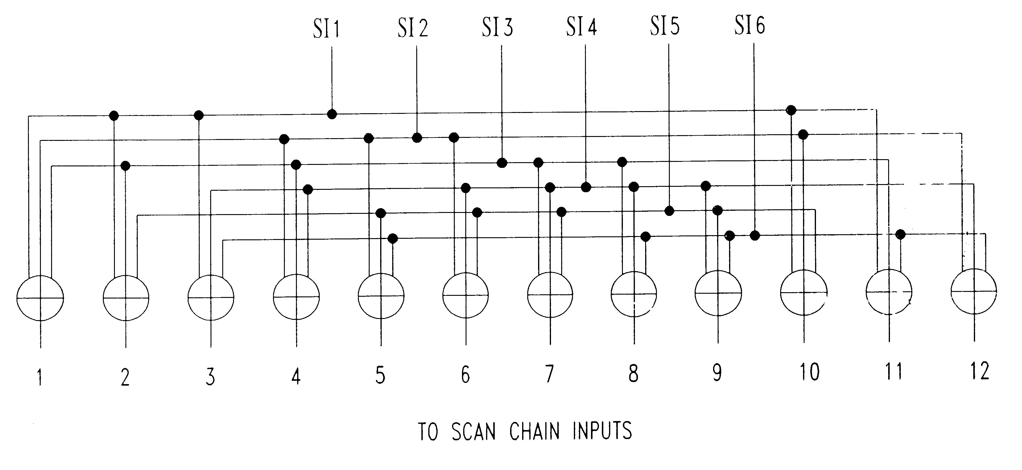
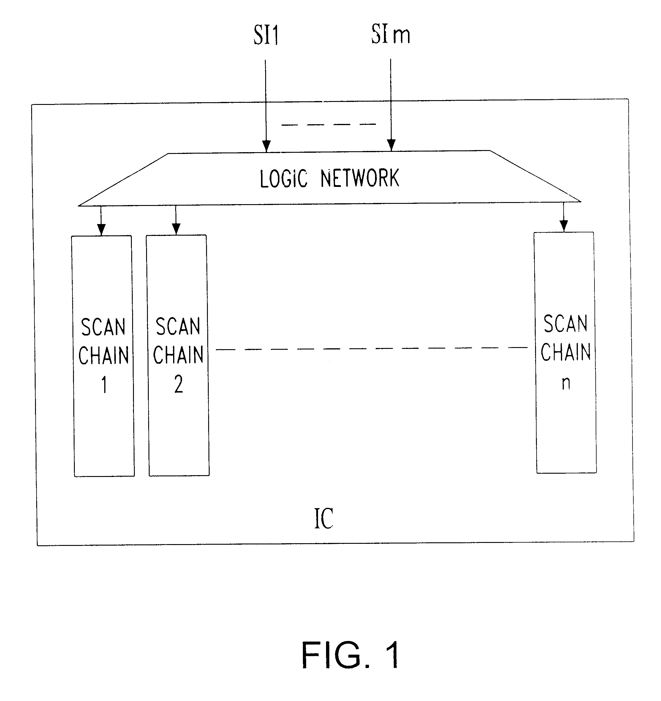
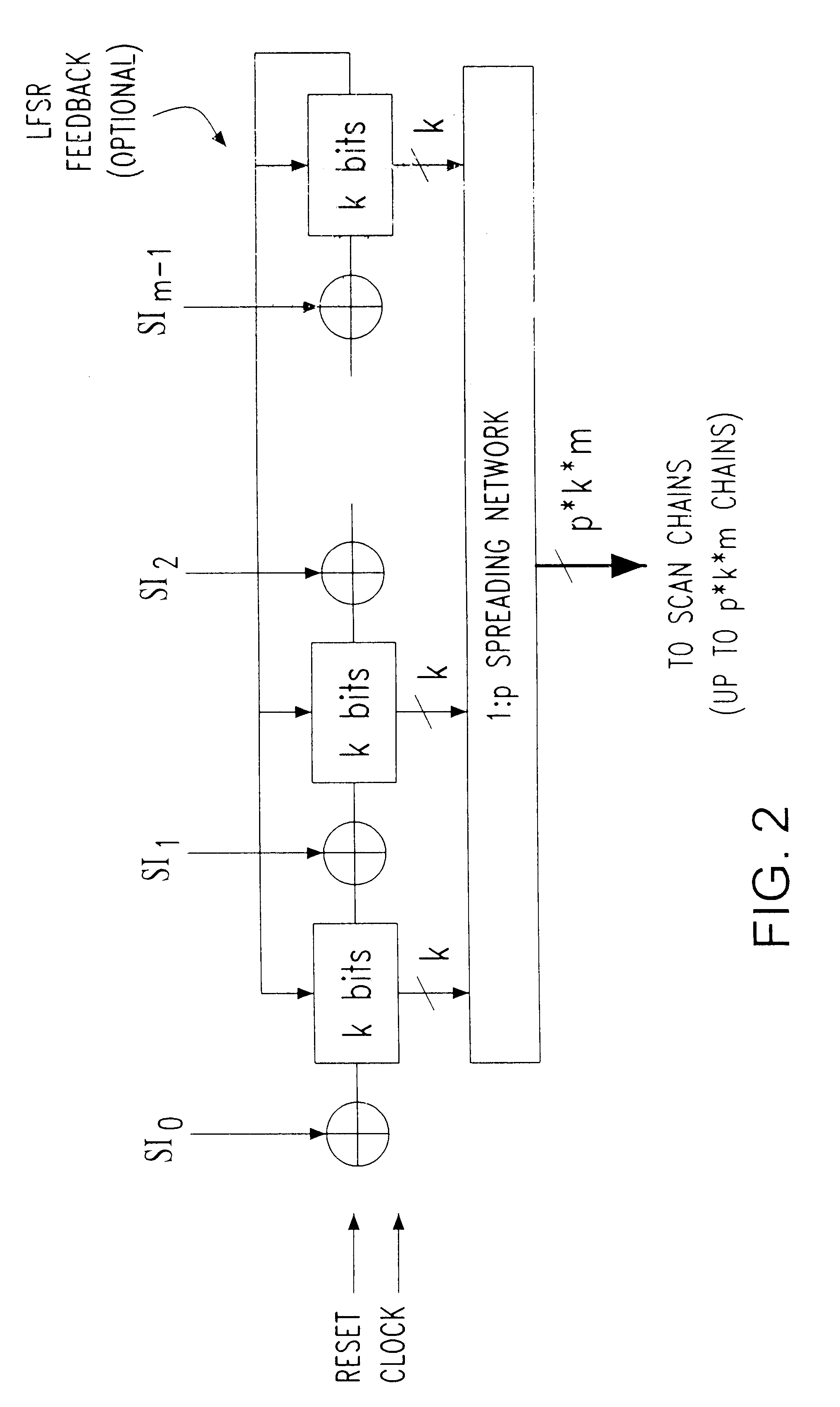
The integrated logic network (i.e., decoder) makes it possible to replace the fully expanded, ready-to-use test stimulus data used for conventional scan testing in the ATE with a more compact encoded data. Only the much smaller amount of encoded data is stored in the archival storage from where it is transferred and loaded into the ATE buffer memory without prior decoding the data. The ATE delivers the test stimulus data in its compact encoded form to the scan PIs of the circuit under test without any additional data transformations performed by the ATE. No special software and / or hardware support is required by the ATE. The encoded data is expanded in real-time by the integrated decoder within the circuit under test and a fully decoded test stimulus data word is loaded into the internal scan chains with every scan clock cycle.

The integrated decoder network to be described hereinafter is inserted within the circuits under test between a certain number of external scan Primary Inputs...


PUM


Abstract

A method and apparatus for improving the efficiency of scan testing of integrated circuits is described. This efficiency is achieved by reducing the amount of required test stimulus source data and by increasing the effective bandwidth of the scan-load operation. The reduced test data volume and corresponding test time are achieved by integrating a real-time test data decoder or logic network into each integrated circuit chip. The apparatus, servicing a plurality of internal scan chains wherein the number of said internal scan chains exceeds the number of primary inputs available for loading data into the scan chains, includes: a) logic network positioned between the primary inputs and the inputs of the scan chains, the logic network expanding input data words having a width corresponding to the number of the primary inputs, and converting the input data words into expanded output data words having a width that corresponds to the number of the internal scan chains; and b) coupled to the internal scan chains, registers loaded with bit values provided by the expanded output data words while data previously loaded into the scan chains shifts forward within the scan chains by one bit position at a time; wherein a first plurality of the input data words supplied to the primary inputs produce a second plurality of expanded data words that are loaded into the internal scan chains to achieve an improved test coverage.

Description

This invention is related to scan testing of complex digital circuits including integrated circuits (ICs), higher level assemblies and systems using ICs, and more particularly, to a method and apparatus for expanding test patterns applied to a restricted number of product primary inputs to inputs of a larger number of on-product scan chains for the purpose of scan testing.Scan testing of digital circuits, internal sequential or register elements, such as latches, and the like, scattered between combinatorial components are designed in a way that they can be connected to each other in several parallel shift registers called scan chains. The inputs of the scan chains are connected to primary inputs (PIs) of the product under test. Each scan test typically requires that the scan chains be completely loaded with new test data one or more times using a scan load-operation. This loading operation takes place prior to applying a test sequence that exercises the logic connected to the regis...

Claims


Application Information

Patent Timeline
Patent Type & Authority Patents(United States)
IPC IPC(8): G01R31/28G01R31/3185
CPCG01R31/318547
Inventor KOENEMANN, BERNDBARNHART, CARLKELLER, BRION
Owner GOOGLE LLC
Why Eureka
Try Eureka