Liquid crystal light modulating device and a method for manufacturing same

a technology of light modulating device and liquid crystal, which is applied in the direction of optics, instruments, non-linear optics, etc., can solve the problems of reducing display quality, difficult and difficulty in regulating uniformity, so as to achieve high-quality displays

Inactive Publication Date: 2003-11-18
MINOLTA CO LTD
View PDF12 Cites 41 Cited by
  • Summary
  • Abstract
  • Description
  • Claims
  • Application Information

AI Technical Summary

Benefits of technology

In view of the previously described disadvantages, an object of the present invention provides a liquid crystal light modulating d

Problems solved by technology

Heretofore, it has been difficult to regulate sufficient uniformity of the inter substrate gap within a light modulation range, with resultant disadvantages including display defects which make it difficult to achieve high quality displays.
In ferrodielectric liquid crystals, irregularities in the inter substrate gap cause irregularities in the orientation of the liquid crystals which reduces the display quality.
When driving an element which has a memory such as cholesteric liquid crystals, the display irregularities become pronounced due to the reduced threshold characteristics.
Furthermore, a large amount of the spacers are wastefully removed from the substrate during the photolithographic method.
In addition, productivity is low due to the extreme complexity of the various processes such as the required developing process.
Since only part of the surface coating layer of the spacers comes into contact with the substrate, adequate adhesion cannot be obtained.
Since the spacers themselves are small it is difficult to accurately arrange these spacers at optional positions, essentially making it difficult to eliminate display irregularities.
As a result, the locations of such flocculation readily produce defects in the orientation of the liquid crystal, and produce regions where light is unmodulated such that a display of sufficiently high quality cannot be obtained.
However, sufficient adhesion force is not obtained even when both substrates are adhered inasmuch as the cross section area of the spacers is too small.
Furthermore, in general, ultraviolet-curing resin is soft when in an uncured state, such that when the two substrates are overlaid, even a slight dislocation of th

Method used


Image

  • Liquid crystal light modulating device and a method for manufacturing same
  • Liquid crystal light modulating device and a method for manufacturing same
  • Liquid crystal light modulating device and a method for manufacturing same

Examples


second embodiment (

FIGS. 4.about.15)

In the second embodiment, we describe the structure and method of manufacturing a liquid crystal display device 20 for display an image by switching ON / OFF a plurality of pixels.

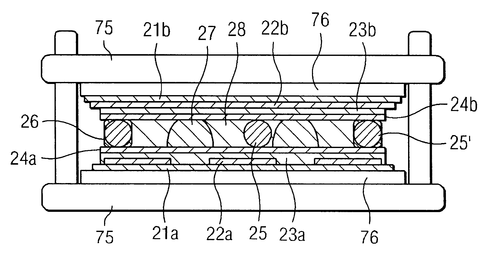
FIG. 4 shows a cross section view of the liquid crystal display device 20. A liquid crystal material 28 is filled between a pair of substrates 21a and 21b as a light modulating layer. Transparent electrodes 22a and 22b are formed in a matrix layout on the substrates 21a and 21b, and insulating layers 23a and 23b and orientation layers 24a and 24b are formed over the transparent electrodes as desired. Spacers 25 are provided between the substrates 21a and 21b to maintain the inter substrate gap. The edges of the substrates 21a and 21b are adhered by a resin seal 26 containing the spacers 25'. In the display region is arranged a resin structure 27 adhered to the substrates 21a and 21b, so as to support the substrates 21a and 21b.

In the liquid crystal display device 20, the points of intersecti...

example 2

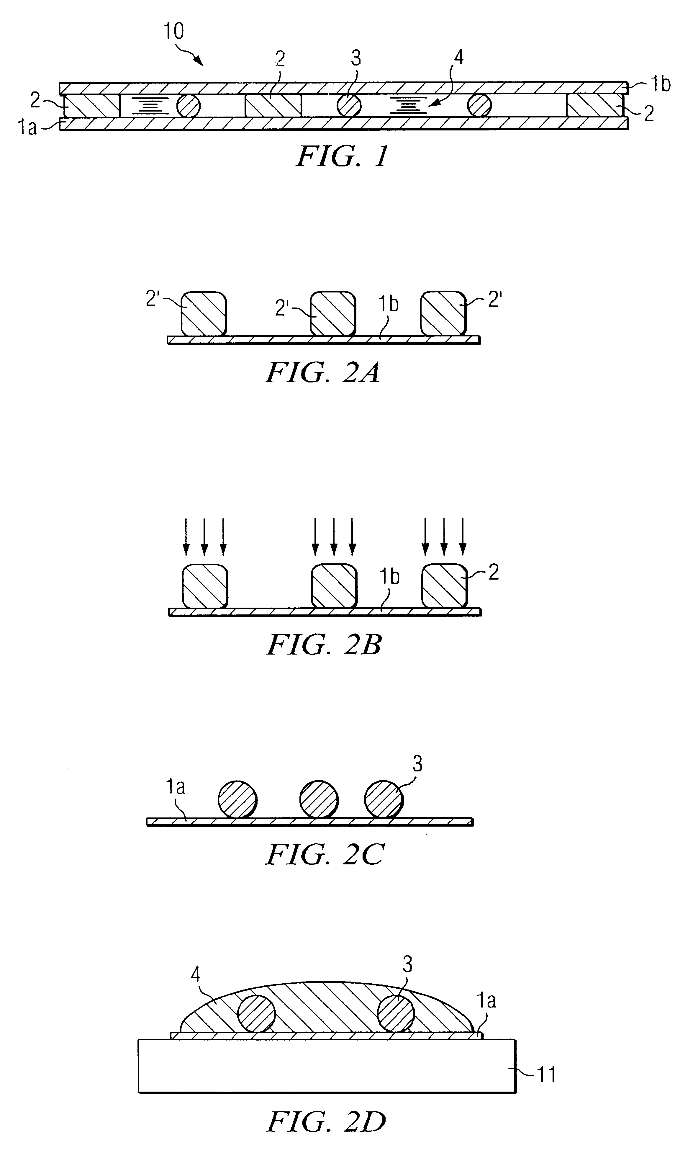
The previously mentioned glass 7059 was used as a first substrate on which an ITO (indium tin oxide) layer 200 nm in thickness was formed by a spattering method. A flexible transparent conductive film FST-5352 (Sumitomo Bakelite Co., Ltd.) was used as the second substrate. This substrate also had an ITO layer formed thereon. The ITO on these substrates was subjected to photolithographic processing to form a band like transparent electrode pattern with an electrode pitch of 350 .mu.m and an electrode width of 300 .mu.m.

Then, a thin film 1000 angstroms in thickness was formed on the transparent electrodes of both substrates via a spin coat method using polysilazane L120 (Tonen Corp.), the substrates were heated for 2 hr at 120.degree. C. in a thermoregulated bath, then an insulating layer was formed by heating for 3 hr in a thermal and moisture regulated bath at 85% humidity. Next, a thin film only 500 angstroms in thickness was formed on the insulating layer of both substrates via a ...

example 3

Example 3 is a liquid crystal display device produced using a resin structure formed of a thermosetting curable resin material. In other aspects, example 3 is identical to example 2, and only the dissimilar aspects are described below.

A thermosetting epoxy resin material, XN21-S (Mitsui Chemicals Co., Ltd.; glass transition temperature 138.degree. C.) was used as the curable resin material. After printing the resin material using a screen identical to that used in example 2, the substrates were heated in a thermoregulated bath at 150.degree. C. for 90 min to cure the resin. Adhesion of the two substrates was accomplished using the device shown in FIGS. 10.about.13. The surface temperature of the heating roller was set at 160.degree. C.

The liquid crystal display device produced as described above maintained uniform inter substrate gap, and had extremely few display irregularities.


PUM

PropertyMeasurementUnit
Temperatureaaaaaaaaaa
Flexibilityaaaaaaaaaa
Shapeaaaaaaaaaa

Abstract

Disclosed is a liquid crystal light modulating device and method for amufacturing the same. The liquid crystal light modulating device has a plurality of resin columns adhering two substrates between which a liquid crystal material is filled. The resin columns are arranged in a predetermined arrangement within a display region of the device. Each columns is made from a curable resin material as a main component, and forms a macromolecular material having thermoplasticity after curing.

Description

This application is based on Japanese Patent Application No. 10-320959 filed on Nov. 11, 1998, the content of which is hereby incorporated by reference.1. Field of the InventionThis invention relates to a liquid crystal light modulating device using a liquid crystal material interposed between a pair of substrates, and a method for manufacturing same.2. Description of Related ArtConventional light modulating devices are widely known which interpose a liquid crystal material between two substrates and use the liquid crystal material as a light shutter. This type of light modulating device is used, for example, as a display device. This type of display device is used as a display in various devices, foremostly, for example, in notebook style personal computer displays and portable telephone displays. Liquid crystal display devices characteristically are thin in design and have low power consumption, and are widely used in portable devices having a small surface area. In recent years, ...

Claims


Application Information

Patent Timeline
IPC IPC(8): G02F1/13G02F1/1339G02F1/1341
CPCG02F1/1339G02F2202/023G02F1/1341G02F1/13394
Inventor NISHIGUCHI, KENJI
Owner MINOLTA CO LTD
Why Eureka
Try Eureka