Electro-optical device having a symmetrically located contact hole and method of producing the same

a technology of symmetrical location and contact hole, which is applied in the direction of semiconductor devices, radio frequency controlled devices, instruments, etc., can solve the problems of difficult formation of contact holes, inability to etch accurately, and inability to produce the same,

Inactive Publication Date: 2003-12-02
138 EAST LCD ADVANCEMENTS LTD
View PDF10 Cites 87 Cited by
  • Summary
  • Abstract
  • Description
  • Claims
  • Application Information

AI Technical Summary

Problems solved by technology

This makes it difficult to form a contact hole through which the semiconductor layer and the pixel electrode are to be electrically connected to each other.
More specifically, a greater depth of etching correspondingly impairs the etching precision, posing a risk of the semiconductor layer being undesirably penetrated and perforated, although the etching has to be stopped upon reaching the semiconductor layer.
It is therefore extremely difficult to form such a deep contact hole by a dry etching process alone.
One solution is to use both dry etching and wet etching in combination, but such a solution inevitably enlarges the diameter of the contact hole due to the use of the wet etching process, making it difficult to lay out necessary wiring and electrodes in restricted areas available on the substrate.
Consequently, the green light G undergoes turns of a number which is smaller by one than the number of turns sustained by the red and blue light rays R and B. Obviously, this problem occurs when the optical system is arranged such that the R light or the B light, rather than the G light, pass through the prism without being reflected.
The same problem is encountered also when the light rays of the three colors are synthesized into the projected light by means of an optical element used as a substituent for the prism 502, e.g., a dichroic mirror.
Implementation of micro-fine pixel pitch, however, poses another problem: namely, since the production technique limits refining of geometric factors such as electrode size, line width and contact-hole diameter, the pixel aperture ratio is undesirably reduced when the pixel pitch is made smaller, as a result of increase of the ratio of the area occupied by the lines, electrodes and so on.
Another problem accompanying the micro-finer pixel pitch is as follows.
From the view point of production technique, there also is a limit in the reduction of thicknesses of the TFTs and conductive layers such as those serving as data lines, scanning lines and capacitance lines, as well as thicknesses of intervening inter-layer insulation films.
Such a solution, however, excessively reduce the area of the aperture region in each pixel, thus posing another problem.
In particular, production of a multi-plate-type color projector, employing three units of electro-optical device having a very fine pixel pitch, suffers from a very high rate of production of defective products.
Similarly, a multi-plate-type color projector having three units of electro-optical device having a very fine pixel pitch suffers from very heavy deterioration of the image due to disclination attributable to the presence of a step on the surface of each pixel electrod...

Method used


Image

  • Electro-optical device having a symmetrically located contact hole and method of producing the same
  • Electro-optical device having a symmetrically located contact hole and method of producing the same
  • Electro-optical device having a symmetrically located contact hole and method of producing the same

Examples


first embodiment

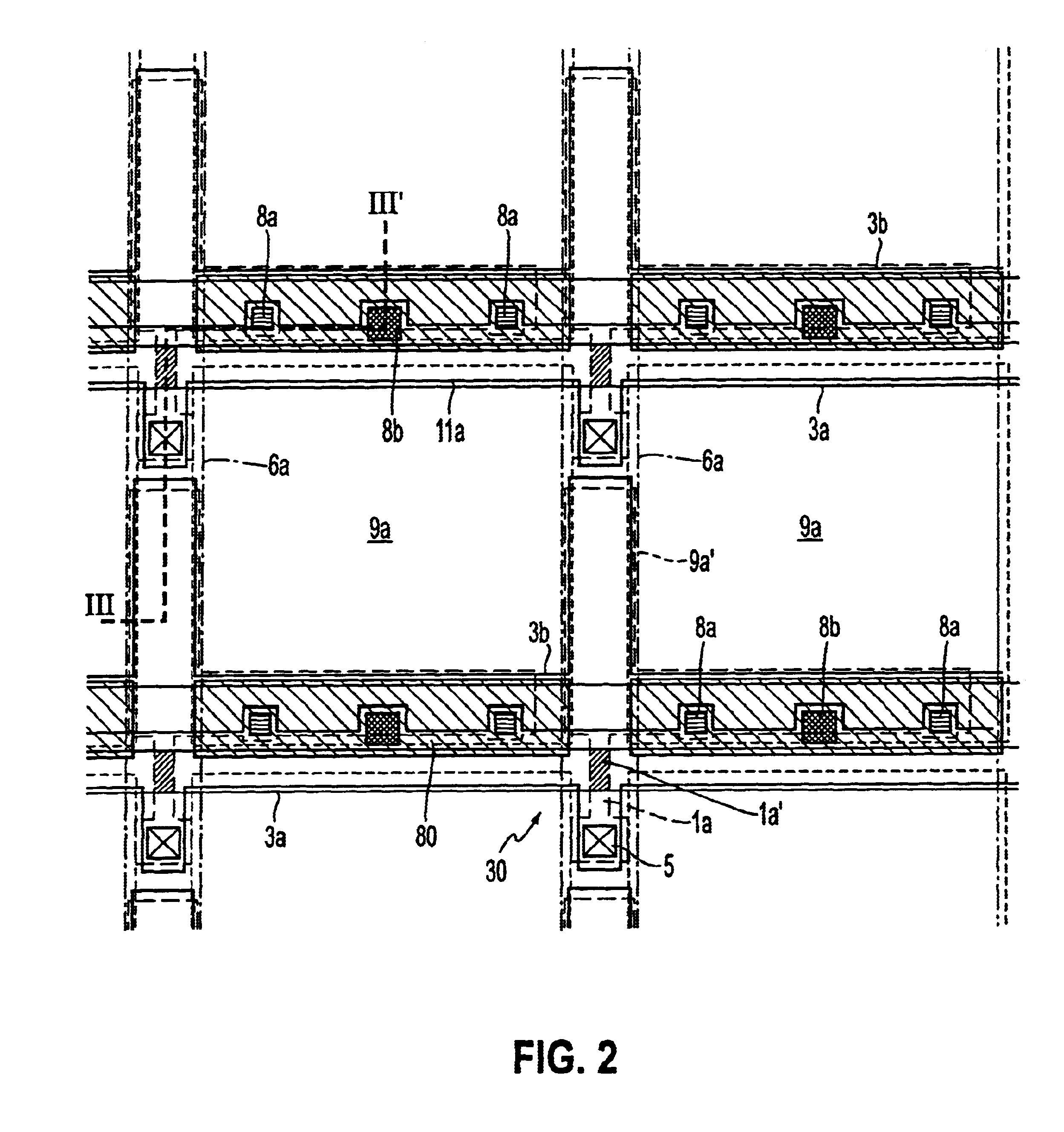
Process of Producing First Embodiment of the Electro-optical Device

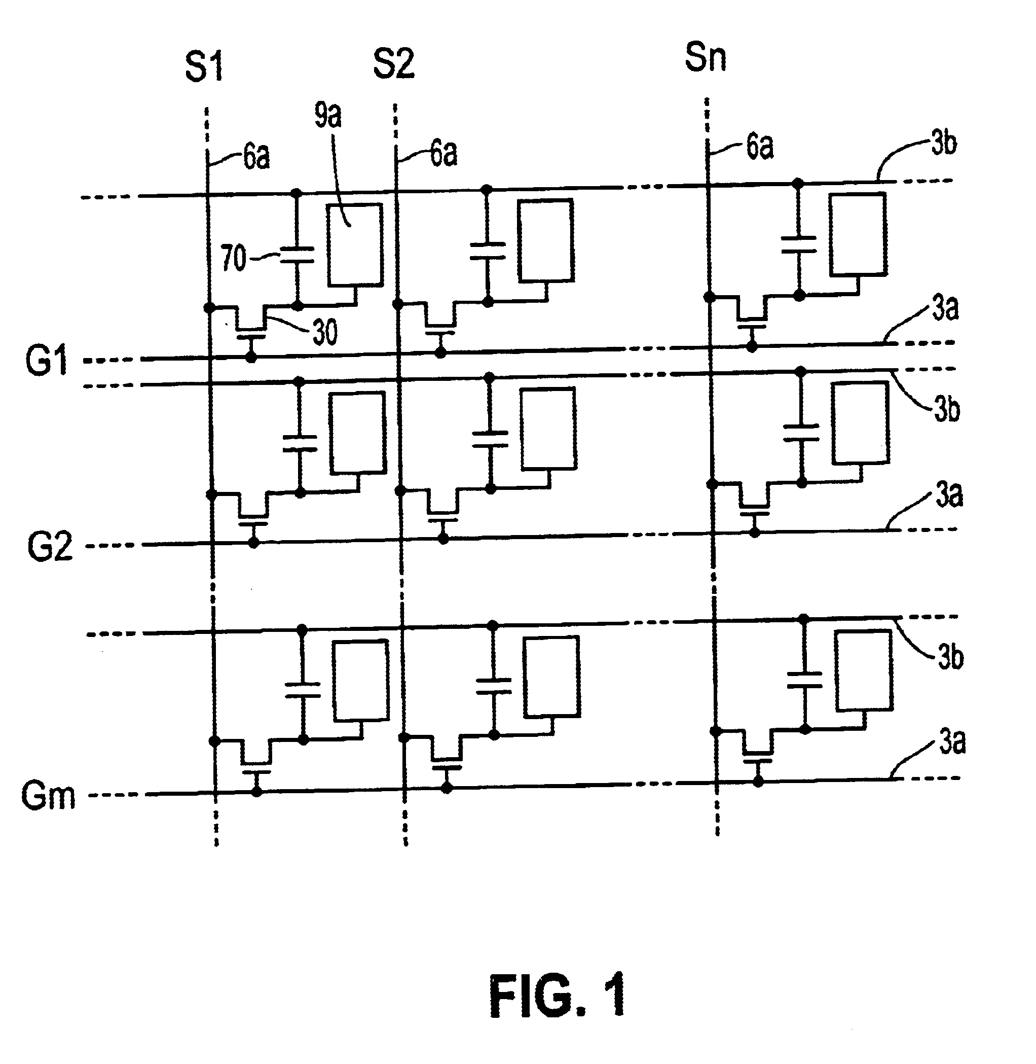
A description will now be given of a process for producing the liquid crystal device of the embodiment having the described structural features, with reference to FIGS. 4 to 7. In FIGS. 4 to 7, the layers on the TFT array substrates are shown at different steps of the process, in sectional views similar to that shown in FIG. 3, i.e., in a sectional view taken along the line III--III of FIG. 2.

Referring first to FIG. 4, in particular Step (1), a TFT array substrate is prepared from, for example, quartz glass, hard glass or silicon. Preferably, the TFT array substrate is heat-treated at a high temperature of about 900.degree. C. to about 1300.degree. C. in an inert gas atmosphere such as of N.sub.2 (nitrogen). This pre-treatment reduces any distortion or strain of the TFT array substrate 10 which may be caused in subsequent high-temperature process. More specifically, the pretreatment is conducted by heating the TFT ar...

second embodiment

of Electro-optical Device

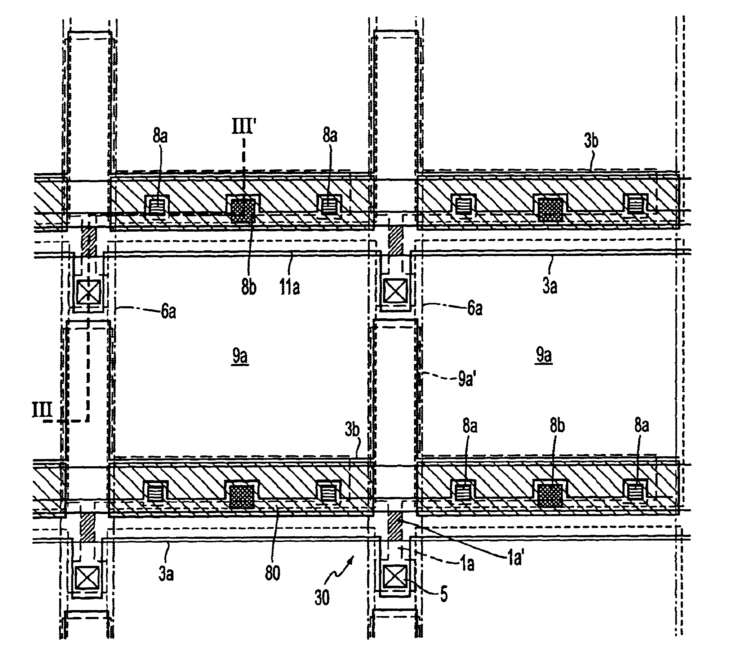
A description will now be given of a liquid crystal device which is a second embodiment of the electro-optical device of the present invention, with specific reference to FIG. 8. FIG. 8 is a plan view of a TFT array substrate used in the second embodiment, carrying data lines, scanning lines, pixel electrodes, light-shielding films and so forth formed thereon, showing particularly a group of adjacent pixels. In FIG. 8, components or elements that are the same as those used in the first embodiment shown in FIG. 2 are denoted by the same reference numerals as those employed in the description of the first embodiment, and description of such components or elements is omitted.

Referring to FIG. 8, the contact hole 8a in the second embodiment is formed in the portion of the non-aperture region extending along the scanning line 3a, at the side of the capacitance line 3b contacting the aperture region, unlike the contact hole 8a in the first embodiment. Other portio...

third embodiment

of Electro-optical Device

A description will now be given of a liquid crystal device which is a third embodiment of the electro-optical device of the present invention, with specific reference to FIGS. 9 and 10. FIG. 9 is a plan view of a TFT array substrate used in the third embodiment, carrying data lines, scanning lines, pixel electrodes, light-shielding films and so forth formed thereon, showing particularly a group of adjacent pixels. FIG. 10 is a sectional view taken along the line X--X of FIG. 9. In FIG. 10, layers and elements are shown at different scales of magnification in order to make them recognizable on the Figure. In FIGS. 9 and 10, components or elements that are the same as those used in the first embodiment shown in FIGS. 2 and 3 are denoted by the same reference numerals as those employed in the description of the first embodiment, and description of such components or elements is omitted.

Referring to FIGS. 9 and 10, the third embodiment employs a combination of a...


PUM


Abstract

An electro-optical device such as an active-matrix-driven liquid crystal device is improved to suppress undesirable effects of dents and steps that appear on pixel electrode surfaces due to presence of contact holes that interconnect a semiconductor layer and pixel electrodes through the intermediary of a conductive layer. The liquid crystal device has a TFT array substrate carrying a TFT, data lines, scanning lines, capacitance lines and pixel electrodes. The pixels and TFTs are electrically connected via contact holes through the intermediary of barrier layers. At least each contact hole is formed in a non-aperture region at a position symmetrical with respect to two adjacent data lines.

Description

1. Field of the InventionThe present invention relates to an electro-optical device of the type driven by an active matrix, as well as to the method of producing such an electro-optical device. More particularly, the present invention pertains to a technical field of an electro-optical device having a conductive layer which serves to provide excellent electrical connection between pixel electrodes and pixel-switching thin film transistors (referred to as "TFT", hereinafter), and also to a method of producing the electro-optical device.2. Description of Related ArtHitherto, an electro-optical device of the type driven by a TFT active matrix has a TFT array substrate on which numeral scanning lines and data lines which run in orthogonal directions in a crossing manner are arranged. Numerous TFTs disposed at the points where the scanning lines and data lines cross each other are also arranged. Each TFT has a gate electrode connected to one of the scanning lines and has a semiconductor ...

Claims


Application Information

Patent Timeline
IPC IPC(8): G02F1/1362G02F1/13
CPCG02F1/136227H01L27/1255H01L29/78633
Inventor MURADE, MASAO
Owner 138 EAST LCD ADVANCEMENTS LTD
Why Eureka
Try Eureka