Stabilization of configurable molecular mechanical devices

a molecular mechanical device and configurable technology, applied in the direction of instruments, non-metal conductors, conductors, etc., can solve the problems of inability to scale well, the level of control is not good, and the implementation cost is extremely high, so as to achieve the effect of stable configuration system

Inactive Publication Date: 2003-12-16
SAMSUNG ELECTRONICS CO LTD
View PDF4 Cites 14 Cited by
  • Summary
  • Abstract
  • Description
  • Claims
  • Application Information

AI Technical Summary

Benefits of technology

The method of the present invention is very general and allows a configuring of arbitrary molecular devices with practically indefinite lifetime (>10 years at room temperature).
The method of the present invention solves the above-noted problem of switching through high energy barriers and allows (i) configuring of the molecular switches and then (ii) making the configured system stable with respect to thermal noise and other external perturbations.

Problems solved by technology

However, because of a combination of physical and economic reasons, the miniaturization that has accompanied the growth of Si ICs is reaching its limit.
The major problem with (1) is that the wafer on which the devices are built must be aligned to within a small fraction of the size of the device features in at least two dimensions for several successive stages of lithography, followed by etching or deposition to build the devices.
This level of control does not scale well as device sizes are reduced to nanometer scale dimensions.
It becomes extremely expensive to implement as devices are scaled down to nanometer scale dimensions.
The major problem with (2) is that it is a serial process, and direct writing a wafer full of complex devices, each containing trillions of components, could well require many years.
Finally, the problem with (3) is that high information content molecules are typically macromolecular structures such as proteins or DNA, and both have extremely complex and, to date, unpredictable secondary and tertiary structures that cause them to twist into helices, fold into sheets, and form other complex 3D structures that will have a significant and usually deleterious effect on their desired electrical properties as well as make interfacing them to the outside world impossible.
In spite of much speculation, however, there are very few experimental results available at this point in time that show some kind of possible switching behavior, the origin of which (intrinsic or extrinsic) is the subject of debate.
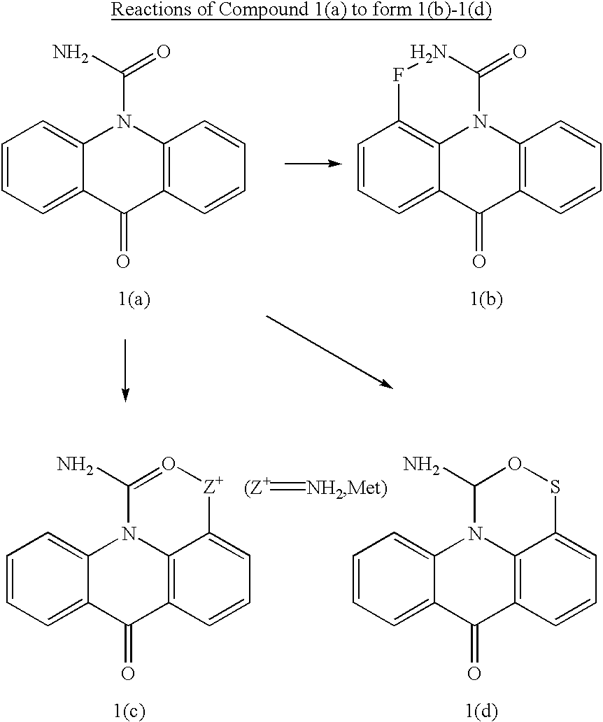
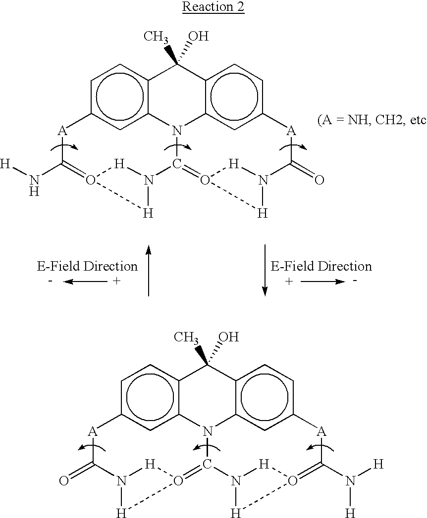
On the one hand, the conformation of stronger bonded molecules is difficult to change, and requires an application of even stronger fields, which in the case of the hydrogen bond are already comparable to atomic fields (.about.10.sup.+8 to 10.sup.+9 V / cm), and can easily damage the device.
On the other hand, the barrier of 0.5 eV is insufficient for any reasonable application, since the corresponding lifetime is short with respect to thermal fluctuations destroying the given configuration of the switch.

Method used


Image

  • Stabilization of configurable molecular mechanical devices
  • Stabilization of configurable molecular mechanical devices
  • Stabilization of configurable molecular mechanical devices

Examples


Embodiment Construction

Definitions

As used herein, the term "self-aligned" as applied to "junction" means that the junction that forms the switch and / or other electrical connection between two wires is created wherever two wires, either of which may be coated or functionalized, cross each other, because it is the act of crossing that creates the junction.

The term "self-assembled" as used herein refers to a system that naturally adopts some geometric pattern because of the identity of the components of the system; the system achieves at least a local minimum in its energy by adopting this configuration.

The term "singly configurable" means that a switch can change its state only once via an irreversible process such as an oxidation or reduction reaction; such a switch can be the basis of a programmable read-only memory (PROM), for example.

The term "reconfigurable" means that a switch can change its state multiple times via a reversible process such as an oxidation or reduction; in other words, the switch can...


PUM

PropertyMeasurementUnit
angleaaaaaaaaaa
energy barrieraaaaaaaaaa
sizeaaaaaaaaaa

Abstract

A route to the fabrication of electronic devices is provided, in which the devices consist of two crossed wires sandwiching an electrically addressable molecular species. The approach is extremely simple and inexpensive to implement, and scales from wire dimensions of several micrometers down to nanometer-scale dimensions. The electronic devices can be used to produce crossbar switch arrays, logic devices, memory devices, and communication and signal routing devices. The construction of molecular electronic devices is achieved on a length scale than can range from micrometers to nanometers via a straightforward and inexpensive chemical assembly procedure. The molecular switchable devices in the cross-bar geometry are configurable while the conformational change is controlled by intramolecular forces that are stronger than hydrogen bonding. The method of the present invention is directed to configuring an ensemble of molecular switches in a prescribed manner in cross-bar geometry and then making such configuration either substantially permanent or stable with respect to temperature fluctuations.

Description

The present invention relates generally to electronic devices whose functional length scales are measured in nanometers, and, more particularly, to simple devices used as building blocks to form more complicated structures, and to the methods for forming such devices. Devices both of micrometer and nanometer scale may be constructed in accordance with the teachings herein.The silicon (Si) integrated circuit (IC) has dominated electronics and has helped it grow to become one of the world's largest and most critical industries over the past thirty-five years. However, because of a combination of physical and economic reasons, the miniaturization that has accompanied the growth of Si ICs is reaching its limit. The present scale of devices is on the order of tenths of micrometers. New solutions are being proposed to take electronics to ever smaller levels; such current solutions are directed to constructing nanometer-scale devices.Prior proposed solutions to the problem of constructing ...

Claims


Application Information

Patent Timeline
Patent Type & Authority Patents(United States)
IPC IPC(8): G02F1/01G02F1/15G02F1/17G11C13/04G11C13/02B82B1/00G11C23/00H01L27/28H01L29/06H01L49/02H01L51/00H01L51/05H01L51/30H01L51/40
CPCB82Y10/00G02F1/174G11C13/02G11C13/041H01L51/006H01L51/0071H01L51/0595G02F1/15Y10S977/943G11C13/04G11C2213/14G11C2213/77G11C2213/81H01L27/285H01L51/0055H10K19/202H10K85/623H10K85/633H10K85/657H10K10/701
Inventor BRATOVSKI, ALEXANDREZHANG, XIAO-ANWILLIAMS, R. STANLEY
Owner SAMSUNG ELECTRONICS CO LTD
Why Eureka
Try Eureka