Semiconductor-on-insulator lateral p-i-n photodetector with a reflecting mirror and backside contact and method for forming the same

a lateral p-i-n and silicon p-i-n technology, applied in the field of photodetectors for optical communication and to a method of forming pin photodiodes, can solve the problems of low quantum efficiency at 850 nm, large absorption length, and two opposite requirements that are more difficult to meet, and achieve the effect of low speed operation or low quantum efficiency of conventional silicon p-i-n photodiodes

Inactive Publication Date: 2003-12-23
GLOBALFOUNDRIES US INC
View PDF12 Cites 93 Cited by
  • Summary
  • Abstract
  • Description
  • Claims
  • Application Information

AI Technical Summary

Problems solved by technology

However, these two opposite requirements are more difficult to meet when the p-i-n photodiode is produced with an indirect bandgap material, where the absorption length is very large.
Thus, a conventional silicon p-i-n photodiode is expected to have low speed operation or to exhibit low quantum efficiency at 850 nm.
First, most known etching processes can only yield a finite aspect ratio between the trench depth and width. For example, a high aspect ratio of 40:1 and a trench width of 0.2 microns yields a trench depth of about 8 microns. For silicon, this would be only about half of the required trench depth.
Even if the trench can be made deep enough, it may be difficult to fill with the conductor material.
This may affect the detector performance and result in a large RC time, where R is the trench series resistance and C is the device capacitance.
However, the detector quantum efficiency is expected to be lower due to the loss of photons that are absorbed below the insulating film.
Thus, the conventional structure of FIG. 2 is problematic as well.
This is problematic.
The structure of FIG. 1 does not achieve such a replication.
However, this structure of FIG. 2 is problematic in its resistance, capacitance, as well as its efficiency, as described above.

Method used


Image

  • Semiconductor-on-insulator lateral p-i-n photodetector with a reflecting mirror and backside contact and method for forming the same
  • Semiconductor-on-insulator lateral p-i-n photodetector with a reflecting mirror and backside contact and method for forming the same
  • Semiconductor-on-insulator lateral p-i-n photodetector with a reflecting mirror and backside contact and method for forming the same

Examples


embodiment

Preferred Embodiment

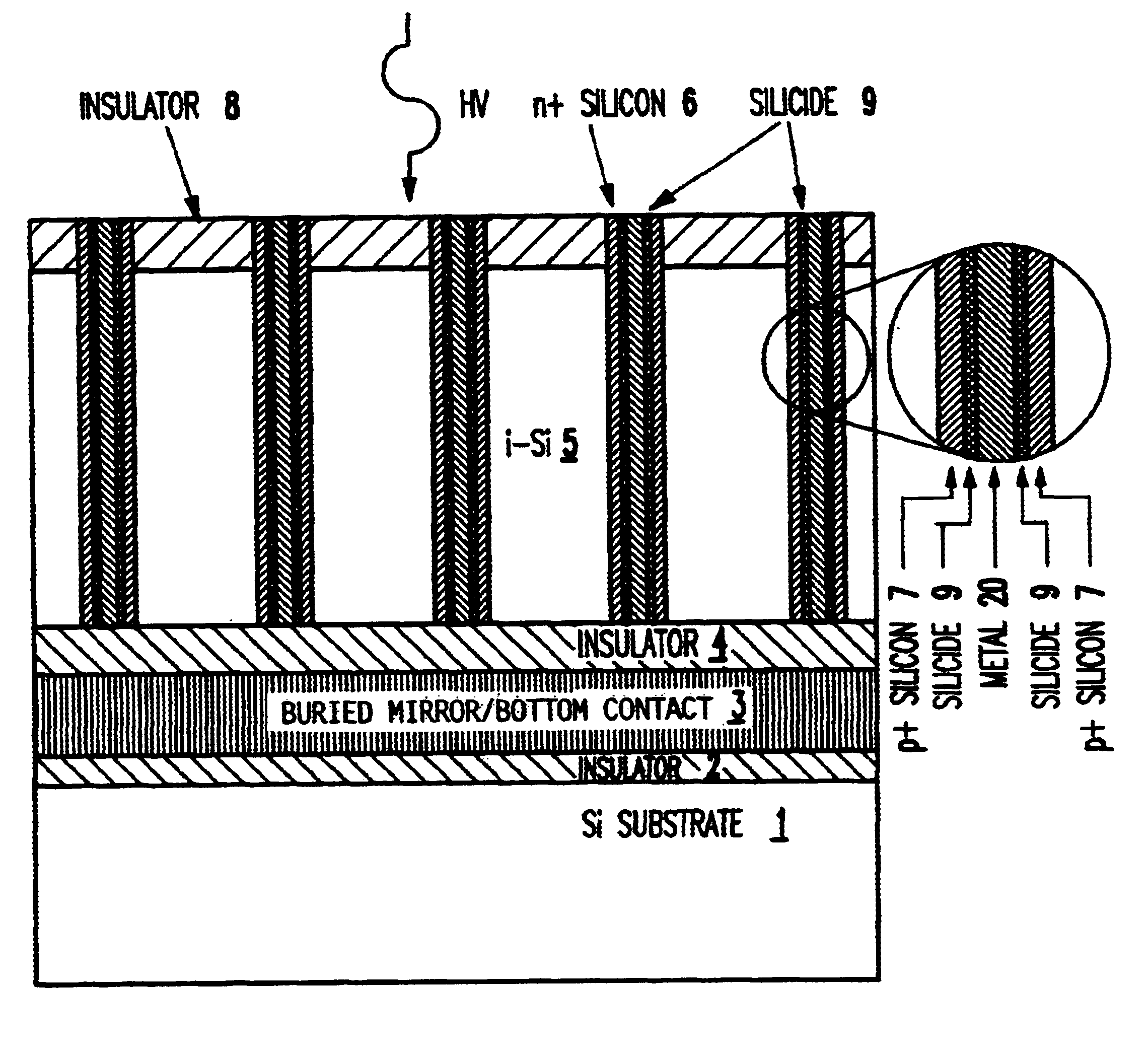
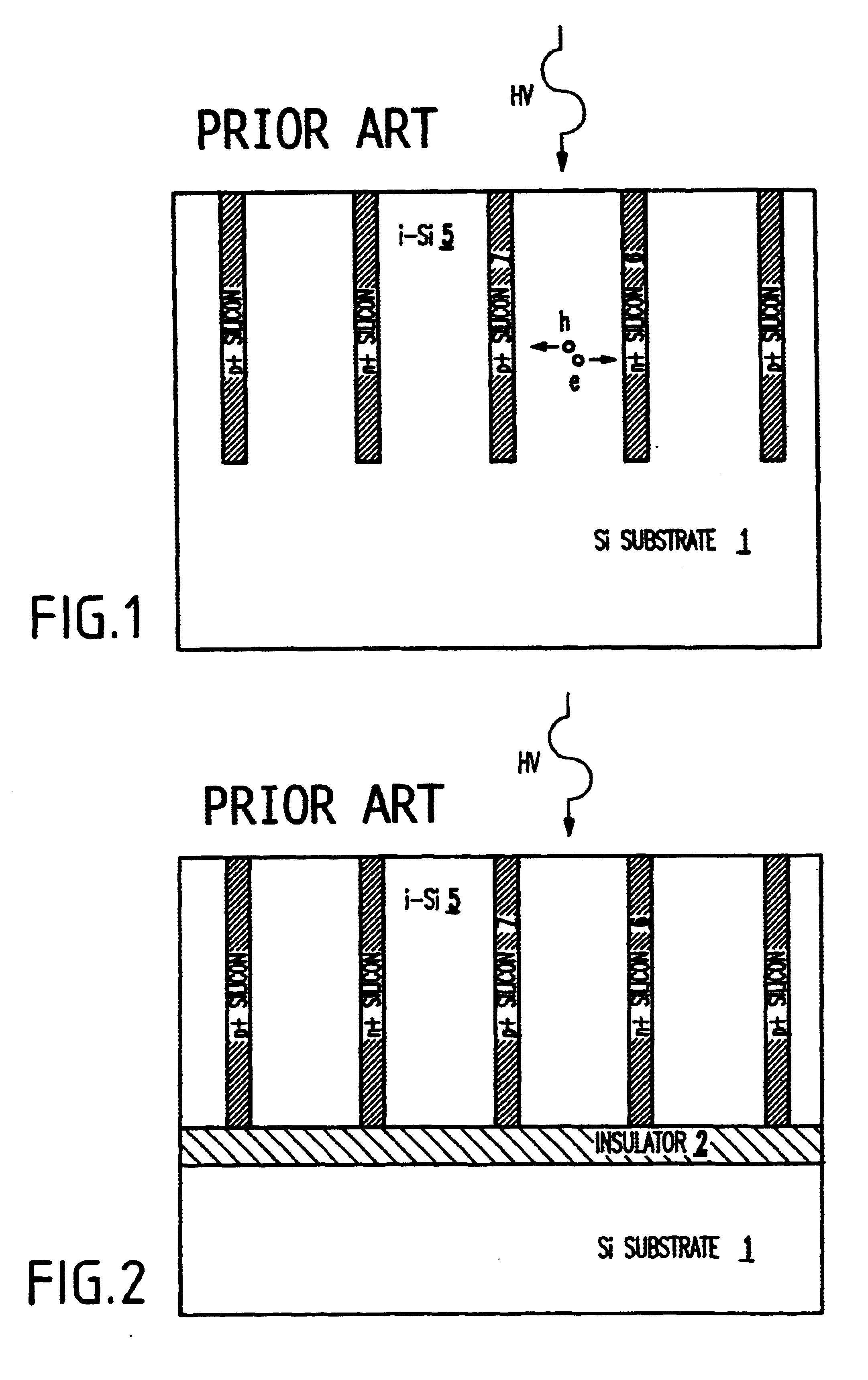
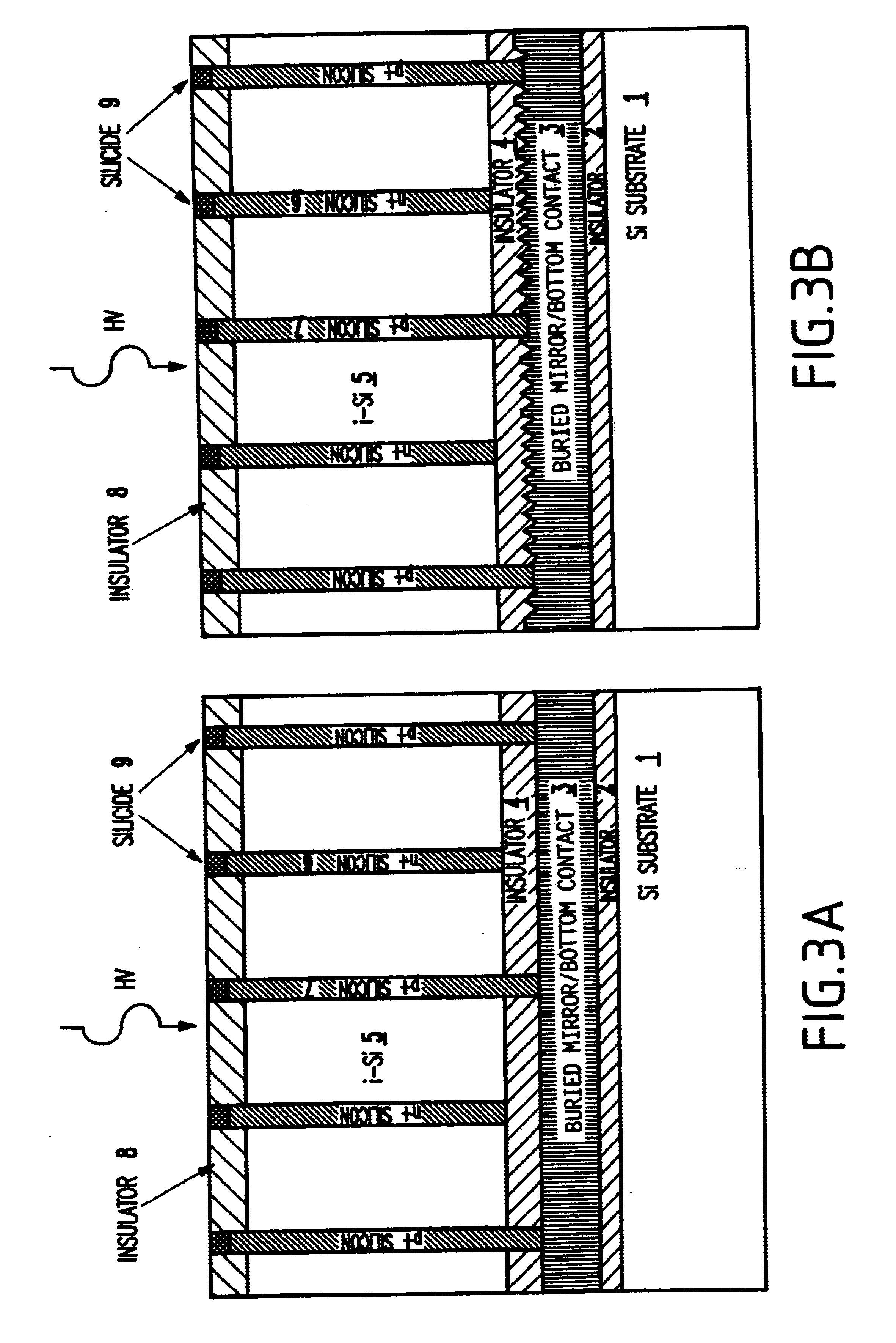
FIG. 3A illustrates a cross section of a structure according to the present invention which includes a silicon substrate 1, a first insulator layer 2 such as oxide, a conductor film 3 such as tungsten (or other metals such as refractory metals that withstand the bonding anneal) or heavily doped poly-Si, a second insulator film 4, an intrinsic silicon-on-insulator layer 5, and alternating n-type 6 and p-type 7 filled trenches.

The contacts to the n-type trenches 6 are made on the top surface, whereas contacts to the p-type trenches 7 are made to the top and to the bottom of each trench 7.

A top view of the detector layout is shown in FIG. 4. The top portion of each trench is converted into silicide 9, such as CoSi.sub.2, to minimize the series resistance from the metal pad 10 to the trench. Such a structure has several advantages over the conventional structures described above and shown in FIGS. 1 and 2.

For example, a sandwich structure, formed by the insulator 4--...

second embodiment

Turning now to FIG. 3D, the present inventors have found that it is desirable to roughen the silicon 5--insulator 4 interface so that the buried mirror 30 (e.g., formed by insulator 4, conductor 3, and insulator 2) is diffusive.

There are several advantages of the diffusive mirror 30 including that a portion of the impinging light would be reflected back into the detector at angles other than perpendicular to the detector surface. Thus, the light's second pass would be longer than the trench depth by 1 / cos(.theta.), where .theta. is the angle by which they diverge from the normal to the surface. If the angle of reflection is large enough, then the light would not escape the silicon film 5 due to total internal reflection.

The configuration of a silicon film 5 on top of a flat mirror will exhibit an etalon effect, such that a destructive interference will result for some wavelengths. Avoiding those dips in the spectrum may be difficult if the silicon film is thick as in the case of the...

third embodiment

FIG. 5 illustrates a cross-section of another trench photodetector 50 embodiment. Photodetector 50 has the following additional features.

That is, the detector 50 is back-illuminated and thus does not require a backside mirror. Instead, a mirror 12 is fabricated (deposited) on top of the wafer surface, which simplifies the fabrication process, since complex mirror bonding steps can be avoided. Mirror 12 may be a metallic mirror or a dielectric mirror which is formed of a multi-layer stack. Such a stack may be formed, for example, from alternating layers of two materials having very different indices of refraction (e.g., polysilicon and oxide, or a nitride and an oxide). The thickness of such layers should be carefully selected since the mirror (unlike a conductor mirror which operates for almost any wavelength) should be tailored to the wavelength of operation.

For example, as shown in FIG. 9, the dielectric mirror can be tailored to be very reflective at 850 nm (which is one of the w...


PUM


Abstract

A photodetector (and method for producing the same) includes a semiconductor substrate, a buried insulator formed on the substrate, a buried mirror formed on the buried insulator, a semiconductor-on-insulator (SOI) layer formed on the conductor, alternating n-type and p-type doped fingers formed in the semiconductor-on-insulator layer, and a backside contact to one of the p-type doped fingers and the n-type doped fingers.

Description

1. Field of the InventionThe present invention generally relates to a photodetector for optical communication and to a method of forming a p-i-n photodiode in a semiconductor.2. Description of the Related ArtA p-i-n diode includes an intrinsic semiconductor layer (i.e., the i-region) that is sandwiched between p-type doped and n-type doped semiconductor layers. The low doping level in the intrinsic region causes this region to be depleted of carriers at low bias. When a reverse bias is applied to the p-i-n diode, most of the high electric field will develop in the intrinsic region.When light is absorbed in the semiconductor, it produces electron-hole pairs. The high electric field serves to separate these carriers. Electrons are swept to the n-type region, where holes are swept to the p-type region. The photogenerated electrons and holes lead to current flow in the external circuit. This current is referred to as the "photogenerated current", or photo-current.For high speed operatio...

Claims


Application Information

Patent Timeline
Patent Type & Authority Patents(United States)
IPC IPC(8): H01L31/06H01L31/058H01L31/0352H01L31/0392H01L31/105H01L31/18
CPCH01L31/03529H01L31/03921H01L31/1804H01L31/105Y02E10/547Y02P70/50
Inventor COHEN, GUY MOSHERIM, KERNROGERS, DENNIS L.SCHAUB, JEREMY DANIELYANG, MIN
Owner GLOBALFOUNDRIES US INC
Why Eureka
Try Eureka