Method of decontaminating process chambers, methods of reducing defects in anti-reflective coatings, and resulting semiconductor structures

a technology of anti-reflective coating and process chamber, which is applied in the direction of solid-state devices, basic electric elements, chemistry apparatus and processes, etc., can solve the problems of non-uniformity on the surface of the layer of silicon nitride, large quantities or magnitudes of in-film particles, etc., and achieve the effect of reducing the degree of distortion in the resultant mask and reducing the exposure of shielded areas

Inactive Publication Date: 2003-12-30
MICRON TECH INC
View PDF21 Cites 76 Cited by
  • Summary
  • Abstract
  • Description
  • Claims
  • Application Information

AI Technical Summary

Benefits of technology

The DARC film fabrication method of the present invention may also include disposing a photoresist over the silicon nitride layer, disposing a diffraction grating between the semiconductor device structure and an electromagnetic radiation source, and directing electromagnetic radiation of a specified wavelength range through the diffraction grating to expose selected areas of the photoresist in order to define a mask therefrom. As is known in the art, the silicon nitride layer and DARC film absorb a significant amount of the electromagnetic radiation (light) that passes through the photoresist. Some of the electromagnetic radiation is, however, reflected back into the photo...

Problems solved by technology

Thus, significantly less "seeding," which may result in the formation of undesirably large quantities or ...

Method used


Image

  • Method of decontaminating process chambers, methods of reducing defects in anti-reflective coatings, and resulting semiconductor structures
  • Method of decontaminating process chambers, methods of reducing defects in anti-reflective coatings, and resulting semiconductor structures
  • Method of decontaminating process chambers, methods of reducing defects in anti-reflective coatings, and resulting semiconductor structures

Examples


Embodiment Construction

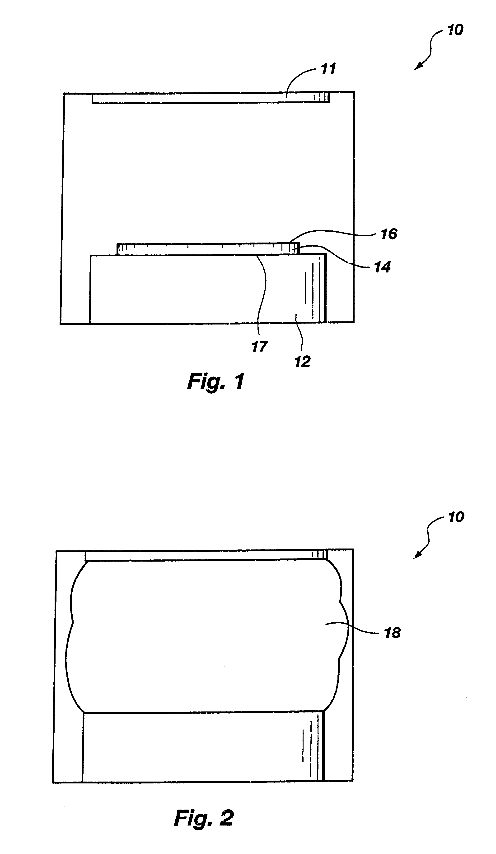
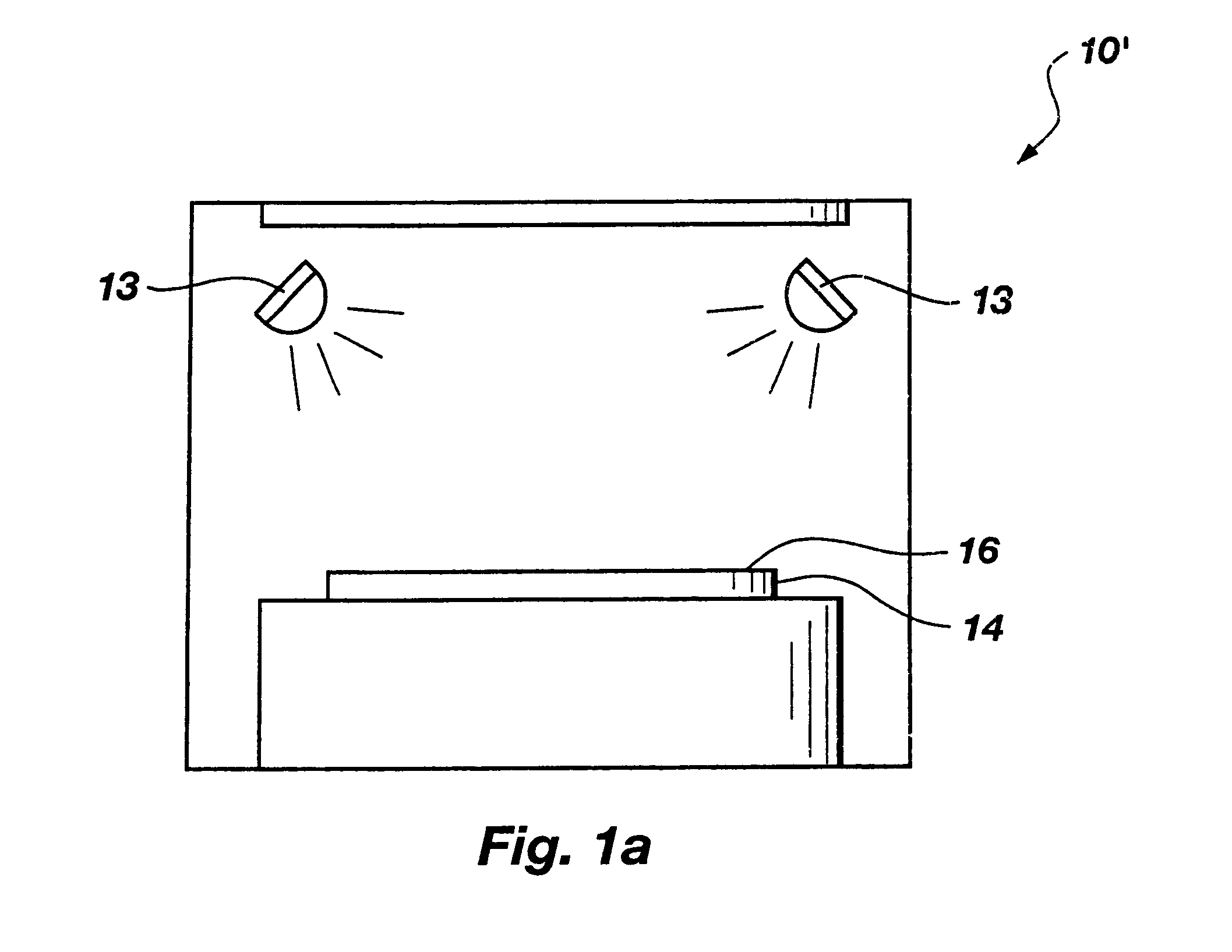
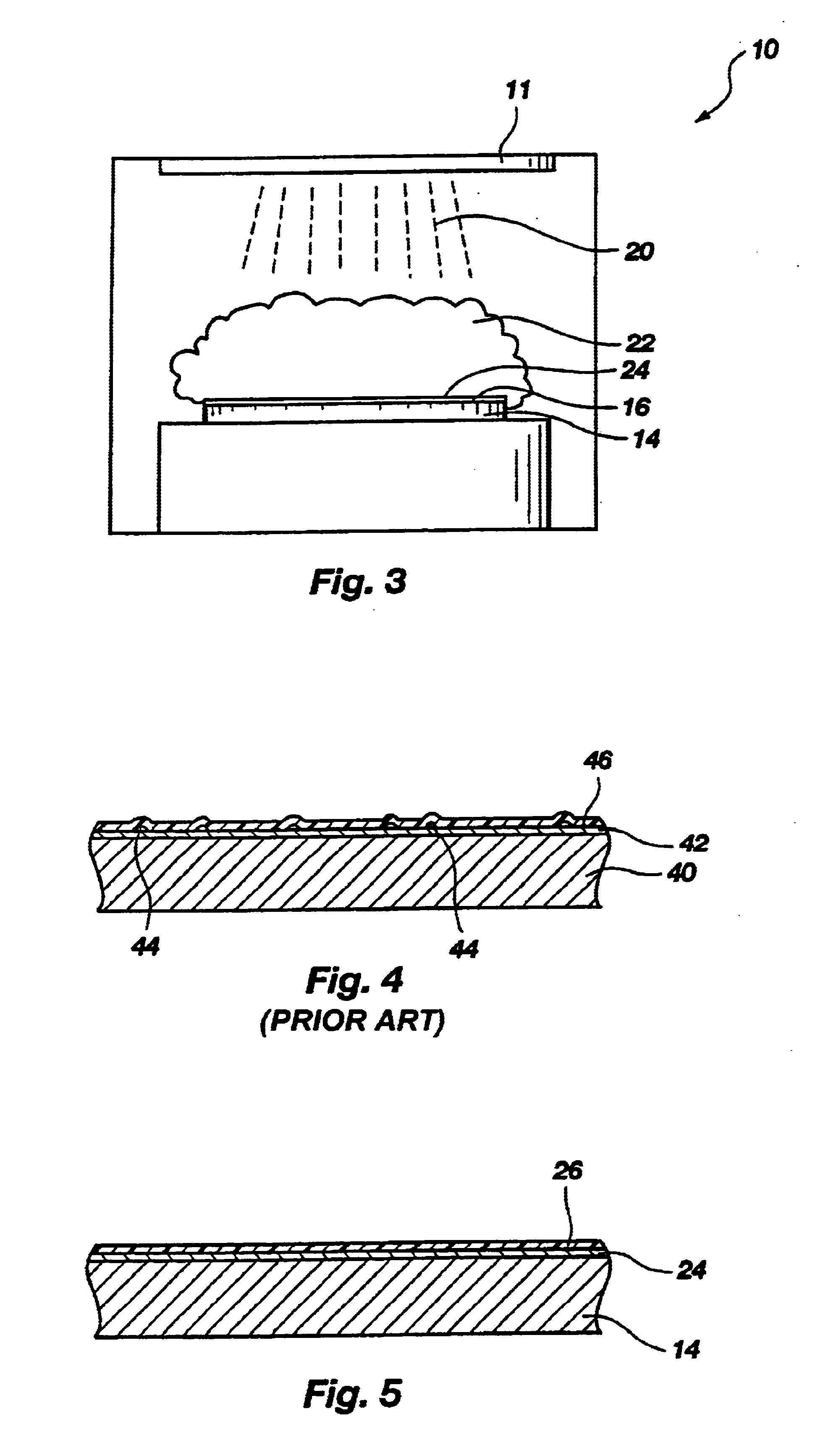
With reference to FIG. 1, a process chamber 10 of a PECVD reactor is illustrated, in which a DARC film including silicon, oxygen and nitrogen is deposited upon a semiconductor device structure. PECVD process chamber 10 includes a source 11 and a wafer support 12, which is also referred to as a susceptor. Preferably, wafer support 12 heats a wafer or other semiconductor device structure 14 disposed thereon from beneath by electrical resistance. Stated another way, an active surface 16 of semiconductor device structure 14, upon which material layers or structures (e.g., DARC films) will be deposited, is heated through the semiconductor device structure by wafer support 12. Exemplary electrical resistance-heated PECVD process chambers in which the DARC film fabrication method and the radio frequency plasma purge process of the present invention may be conducted include, without limitation, the process chamber of a Price DX2 PECVD reactor and the process chambers of other single-wafer a...


PUM

PropertyMeasurementUnit
Surface roughnessaaaaaaaaaa
Thicknessaaaaaaaaaa

Abstract

A method for fabricating a substantially smooth-surfaced anti-reflective coating on a semiconductor device structure including generating a plasma from an inert gas in a process chamber in which the anti-reflective coating is to be deposited. The anti-reflective coating may include silicon, oxygen and nitrogen, and is preferably of the general formula Si.sub.x O.sub.y N.sub.z, where x equals 0.40 to 0.65, y equals 0.02 to 0.56 and z equals 0.05 to 0.33. Preferably, x+y+z equals one. The method may also include fabricating a silicon nitride layer over the anti-reflective coating. A semiconductor device which includes a silicon nitride layer over the anti-reflective coating has a density of less than about 40,000 particles or surface roughness features in the silicon nitride of about 120-150 nanometers dimension per eight inch wafer. Accordingly, a mask that is subsequently formed over the silicon nitride layer has a substantially uniform thickness and is substantially distortion-free.

Description

BACKGROUND OF THE INVENTION1. Field of the InventionThe present invention relates to a method of disposing an anti-reflective coating (ARC), such as a dielectric anti-reflective coating (DARC), on a semiconductor device structure. Particularly, the present invention relates to a process for reducing the occurrence of particles or roughness on an exposed surface of an ARC or a DARC. More particularly, the present invention relates to a process which reduces the incidence of in-film particles and interfacial irregularities between an ARC or DARC layer and an adjacent, overlying silicon nitride layer.2. State of the ArtPhotolithography processes that have been conventionally employed in the manufacture of semiconductor devices typically include disposing a photoresist material over a layer of a semiconductor device structure, such as a wafer or bulk semiconductor material, that is to be patterned, positioning a diffraction grating over the layer of photoresist material, positioning a m...

Claims


Application Information

Patent Timeline
IPC IPC(8): H01L21/02H01L23/52H01L21/027H01L23/532H01L21/314
CPCH01L21/0276H01L23/5329Y10S438/905H01L21/3145H01L2924/0002H01L21/02274H01L21/0214H01L21/022H01L21/0217H01L2924/00
Inventor YIN, ZHIPING
Owner MICRON TECH INC
Why Eureka
Try Eureka