Nonvolatile semiconductor storage device with limited consumption current during erasure and erase method therefor

a semiconductor storage device and non-volatile technology, applied in semiconductor devices, digital storage, instruments, etc., can solve the problems of reducing the current efficiency of the erase operation, generating holes, deteriorating the reliability of the memory cell, etc., and achieve the effect of high efficiency

Inactive Publication Date: 2003-12-30
SHARP KK
View PDF2 Cites 15 Cited by
  • Summary
  • Abstract
  • Description
  • Claims
  • Application Information

AI Technical Summary

Benefits of technology

Accordingly, the object of the present invention is to provide a nonvolatile semiconductor storage device capable of quantitatively estimating the required erase time and the peak value of an erase current, suppressing an increase in the erase time and reducing the erase current and a storage contents erase method therefor. The present invention also provides a method capable of efficiently executing the erase of a plurality of blocks.
In this embodiment, memory arrays within a block targeted for erase can be erased with high efficiency.

Problems solved by technology

The BTBT current not only reduces the current efficiency of the erase operation but also generates a hole, becoming an important factor to deteriorate the reliability of the memory cell.
Since the sources of all the memory cells in a block are connected to an identical source line in the flash memory in which the block batch erase is executed, an increase in the peak current due to the BTBT current becomes a serious problem.
In addition, with regard to the flash memory, due to the fact that the device operable on a single power supply voltage is mainly used for the sake of improvement in operability and the fact that the power supply employed in portable equipment on the big market of the flash memory is limited, it is often the case where a voltage boosted from the power supply voltage by a charge pump circuit is used as a source voltage to be used for source erase.
Therefore, an increase in the consumption current due to the BTBT current becomes still more serious problem in accordance with the adoption of a single power supply voltage and a low voltage.
However, during source erase, the consumption current attributed directly to the BTBT current is especially large, and it can be safely said that the greater part of the current that varies on the time base is attributed to the BTBT current.
The current efficiency of the erase operation is very low due to the BTBT current.
However, the erase time of the flash memory is very long (several milliseconds to several seconds), and it is not easy to secure a capacity sufficient for handling a large current for a long time.
Due to this large peak current, it has been difficult to use a flash memory in a system such as portable equipment, which has only a small current supply capacity.
However, due to the necessity of substrate potential control, there is needed a substantial change of the manufacturing process and the control method, which cannot easily be achieved.
However, there is a demerit that the time required for the erase largely increases by simply lowering the source voltage.
However, it is very difficult to quantitatively grasp the correlation between the source voltage and the peak current value if the variations of the process, the deterioration of the memory cells and so on are taken into consideration.
Therefore, it can be qualitatively estimated to reduce the peak current by the soft erase, but a quantitative determination is difficult.
However, when the electric charges lost by the BTBT current cannot be replenished, the source voltage is lowered due to limitations on the consumption current of the booster circuit, and a soft erase state is established.
However, since the source voltage during erase is not specified by this method, it is very difficult to estimate the required erase time.
However, the erase method shown in FIG. 16 has the problems as follows.
That is, the first problem is that the sum total of the BTBT current flowing from the sources of the memory cells is increased by an increase in the number of memory cells to be simultaneously erased, and when the sum of the currents exceeds the current supply capacity of the booster circuit 1050, the potential of the high voltage 1002 cannot be maintained, hindering the erase operation.
The second problem is that the number of blocks that can be simultaneously erased is limited also by a resistance that accompanies the high voltage 1002.
Furthermore, when the erase voltage is simultaneously applied to the two blocks of the aforementioned four blocks, there inevitably occurs a situation that the voltage drop on the source line exceeds the permissible range no matter which combination is selected.
However, the devising, which requires a change of process, is generally not easy.
Moreover, shortening the source wiring has limitations attributed to the layout arrangement of the blocks and so on.
Moreover, thickening the source wiring width and increasing the switching element capacity lead to an increase in the chip area, and there is a concern about the sacrifice of the chip size and cost.
Therefore, it is unavoidable that a resistance is parasitic on the source line to a certain extent, and this parasitic resistance possibly limits the simultaneous erase of a plurality of blocks.
As described above, there have been limitations on the simultaneous erase of a plurality of blocks due to the current supply capacity of the booster circuit that generates the high voltage applied to the source and the resistance parasitic on the source line.
As described above, according to the conventional source erase method, the peak value of the consumption current during erase is large, and there is a serious hindrance to the use of the method in portable equipment whose current supply capacity is not sufficiently large and the like.
Moreover, according to the method for reducing the peak current by soft erase, it is generally difficult to quantitatively estimate the correlation between the applied source voltage and the peak current value.
Using the technology of limiting the consumption current of the booster circuit is also effective for the suppression of the consumption current, but it is difficult to estimate the time necessary for erase.
Moreover, it has conventionally been difficult to execute batch erase of a plurality of blocks, and when only a single block can be simultaneously erased, the time necessary for erasing a plurality of blocks has been increased roughly in proportion to the number of blocks in which the erase is executed.

Method used


Image

  • Nonvolatile semiconductor storage device with limited consumption current during erasure and erase method therefor
  • Nonvolatile semiconductor storage device with limited consumption current during erasure and erase method therefor
  • Nonvolatile semiconductor storage device with limited consumption current during erasure and erase method therefor

Examples


first embodiment

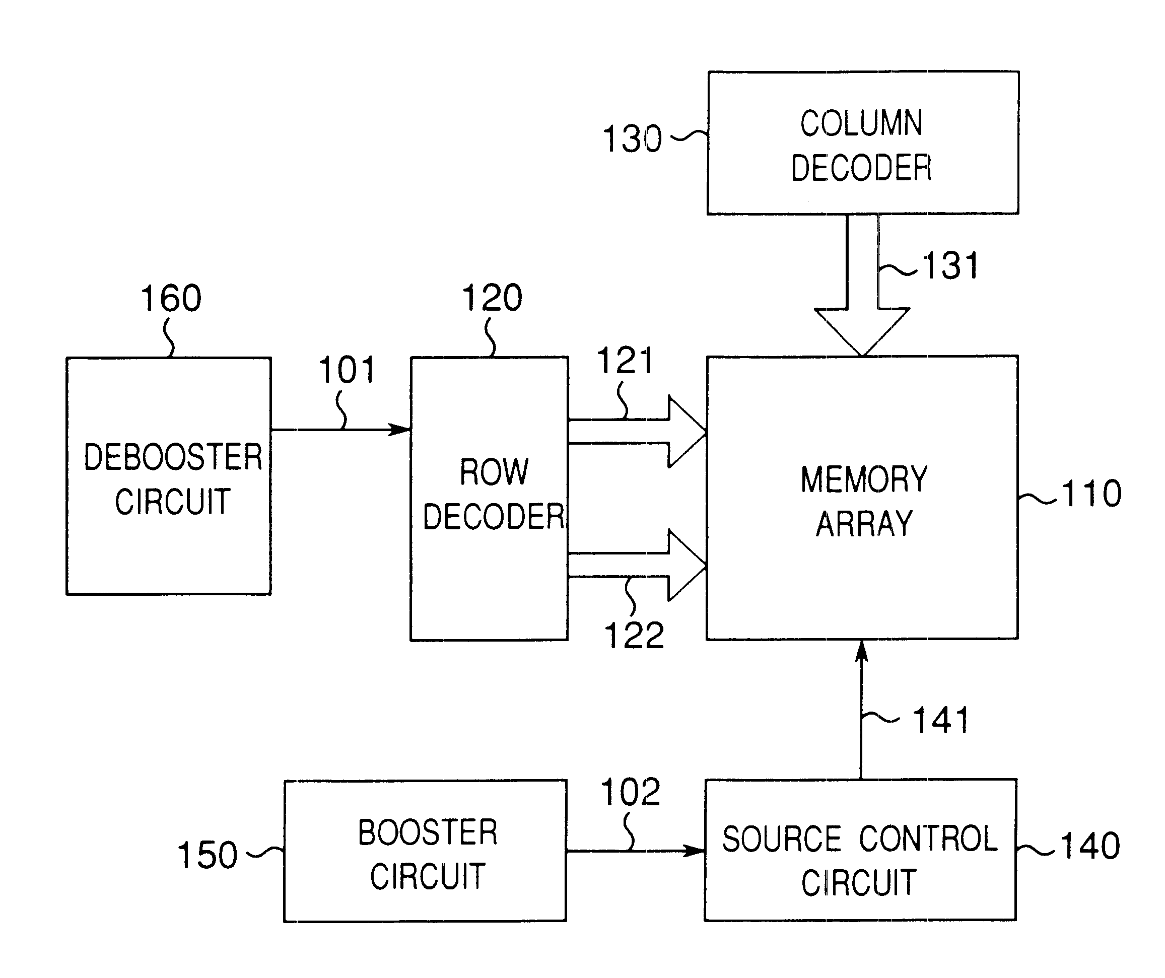
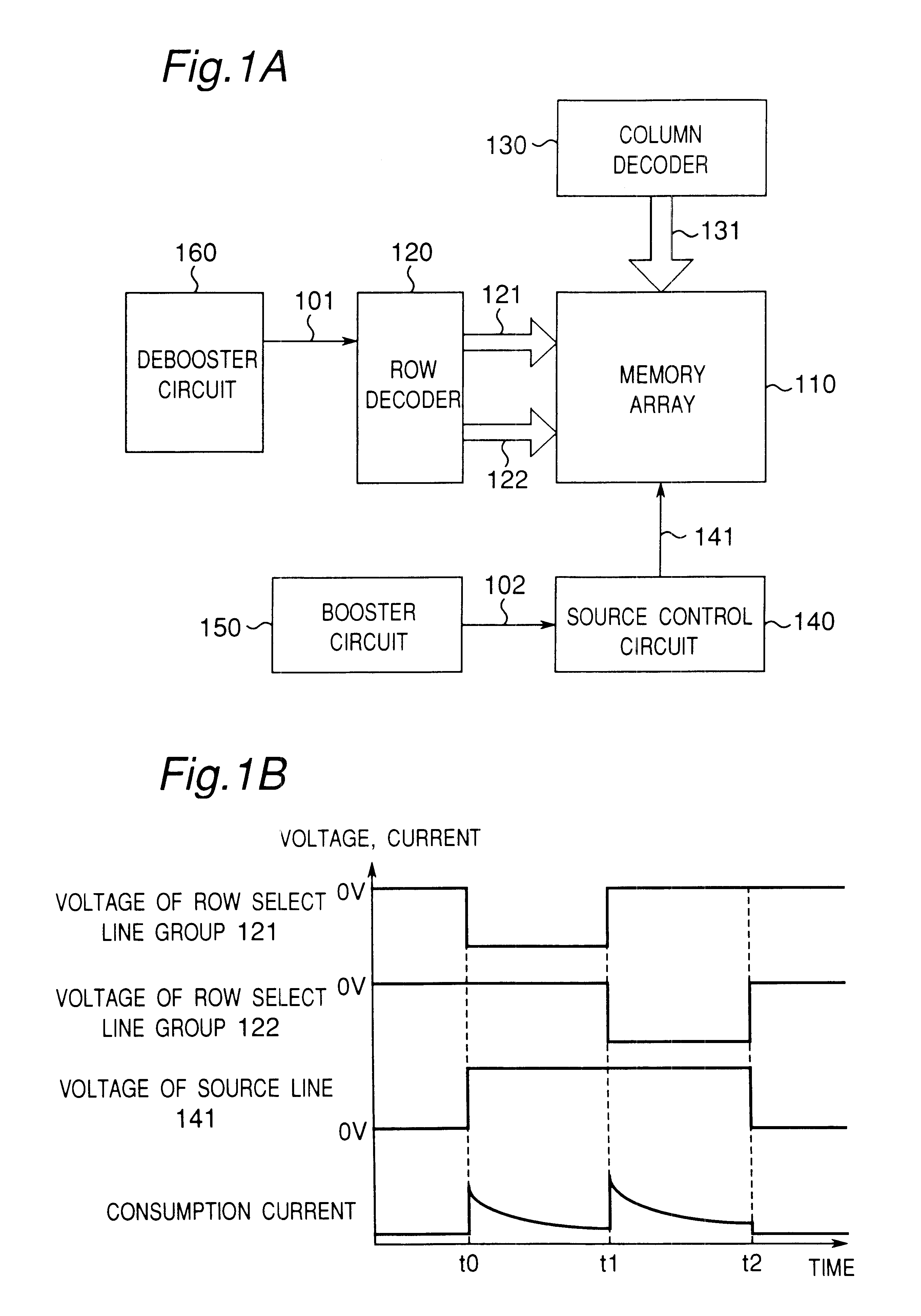
This first embodiment is provided with a memory array 110 that becomes an erase unit, a row decoder 120 for controlling a row select line group 121 and a row select line group 122 and a debooster circuit 160 for generating a negative voltage 101 to be supplied to the row decoder 120. This first embodiment is further provided with a column decoder 130 for controlling a column select line group 131, a source control circuit 140 for controlling a source line 141 and a booster circuit 150 for generating a high voltage 102 to be supplied to the source control circuit 140.

The row select line group 121 and the row select line group 122 are respectively constructed of a plurality of row select lines, while the column select line group 131 is constructed of a plurality of column select lines. Although FIGS. 1A and 1B show an example in which the row select lines connected to the memory array 110 are divided into two row select line groups 121 and 122, it is also possible to further reduce th...

second embodiment

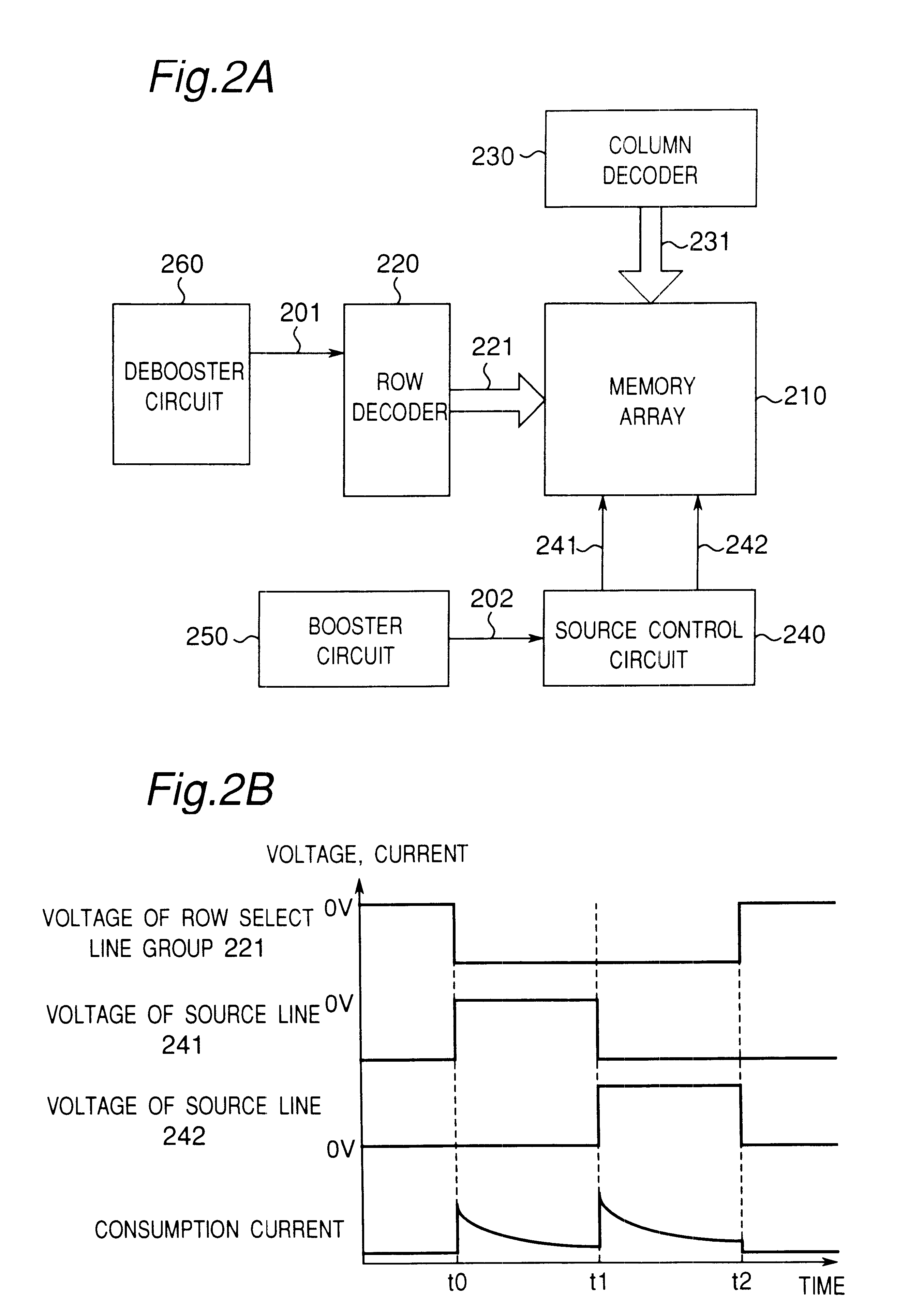
This second embodiment is provided with a memory array 210 that becomes an erase unit, a row decoder 220 for controlling a row select line group 221 and a debooster circuit 260 for generating a negative voltage 201 to be supplied to the row decoder 220. This second embodiment is further provided with a column decoder 230 for controlling a column select line group 231, a source control circuit 240 for controlling a source line 241 and a source line 242 and a booster circuit 250 for generating a high voltage 202 to be supplied to this source control circuit 240.

The row select line group 221 is constructed of a plurality of row select lines, while the column select line group 231 is constructed of a plurality of column select lines. Although the case of two source lines will be described in connection with this embodiment, it is also possible to increase this number, similarly to the division of the row select line group in the first embodiment.

Next, FIG. 3A and FIG. 3B show examples o...

third embodiment

This third embodiment relates to an overerase decision method with the use of the nonvolatile semiconductor storage device of the first or second embodiment.

As shown in the flowchart of FIG. 5, in an erase operation of a flash memory, normally, after an erase voltage is applied (S1, S5), an erase verify (S2, S6) for verifying that the threshold value (threshold voltage) has lowered enough as well as an overerase verify (S3, S7) for verifying that the threshold value has not lowered too much are executed.

If it is found by this erase verify (S2, S6) that threshold values of memory cells (area 1, area 2) have not lowered enough, a further erase voltage is applied (S1, S5). Also, if it is found by the overerase verify (S3, S7) that the threshold values have lowered too much, the threshold values are raised by writing into memory cells in the area 1 and the area 2 that could be in an overerased state (S4, S8).

The storage contents erase method of the third embodiment is constituted by inc...


PUM


Abstract

A nonvolatile semiconductor storage device includes a row decoder which independently controls a plurality of row select line groups. A negative voltage generated by a debooster circuit is applied to individual row select line groups with time shifts. As a result, peaks of erase current can be suppressed, so that consumption current can be reduced. In this device, a current limiting circuit of the booster circuit limits the consumption current of the booster circuit, allowing voltages to be generated within a range under a specified current value according to the conditions of voltage application to the individual row select line groups. Thus, a further reduction of the consumption current at a shorter scale can be achieved.

Description

BACKGROUND OF THE INVENTIONThe present invention relates to a nonvolatile semiconductor storage device that has a means for executing erase in blocks and a storage contents erase method therefor.There has recently been a growing demand for a nonvolatile semiconductor storage device capable of executing erase in blocks, intended mainly for portable equipment.The block erase of a conventional nonvolatile semiconductor storage device capable of executing erase in blocks will be described below with reference to FIGS. 9A, 9B, 10A, 10B, 11, 12 and 13.FIG. 9A shows a typical memory cell structure of an EEPROM (electrically erasable programmable ROM), which is a nonvolatile semiconductor storage device. As shown in this figure, the memory cell has a MOS transistor structure of a two-layer gate constructed of a control gate 701 and a floating gate 702. This memory cell is covered with an insulating film of SiO.sub.2 or the like. This insulating film serves to provide electrical insulation o...

Claims


Application Information

Patent Timeline
Patent Type & Authority Patents(United States)
IPC IPC(8): G11C16/16G11C16/06H01L21/00G11C16/04G11C16/30G11C16/34H01L21/336H01L21/8247
CPCG11C16/0416G11C16/16G11C16/3445G11C16/344G11C16/30H01L29/66825H01L27/11517H10B41/00
Inventor SUMITANI, KENSATOH, TAKAYUKI
Owner SHARP KK
Why Eureka
Try Eureka