Multi-functional micro electromechanical devices and method of bulk manufacturing same

a multi-functional, electromechanical technology, applied in the direction of fluid speed measurement, acceleration measurement using interia forces, instruments, etc., can solve the problems of early failure and time-consuming production process

Inactive Publication Date: 2004-03-16
NASA
View PDF8 Cites 22 Cited by
  • Summary
  • Abstract
  • Description
  • Claims
  • Application Information

AI Technical Summary

Benefits of technology

FIG. 26 is a schematic illustration similar to FIG. 25 illustrating the removal of the Indium Tin Oxi

Problems solved by technology

Because these transducers are made of materials with dissimilar properties, they suffer from coefficient of thermal expansion (CTE) mismatch, which lead

Method used


Image

  • Multi-functional micro electromechanical devices and method of bulk manufacturing same
  • Multi-functional micro electromechanical devices and method of bulk manufacturing same
  • Multi-functional micro electromechanical devices and method of bulk manufacturing same

Examples


Embodiment Construction

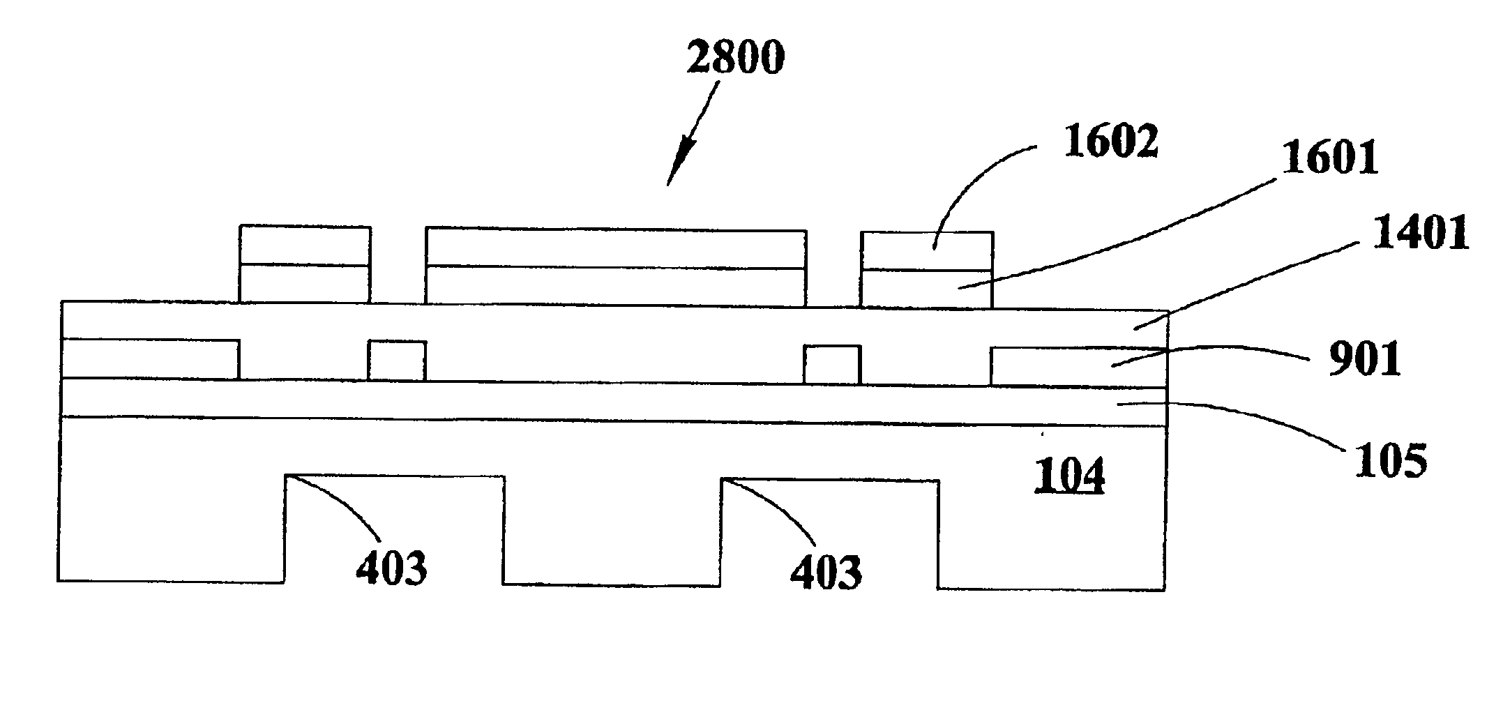
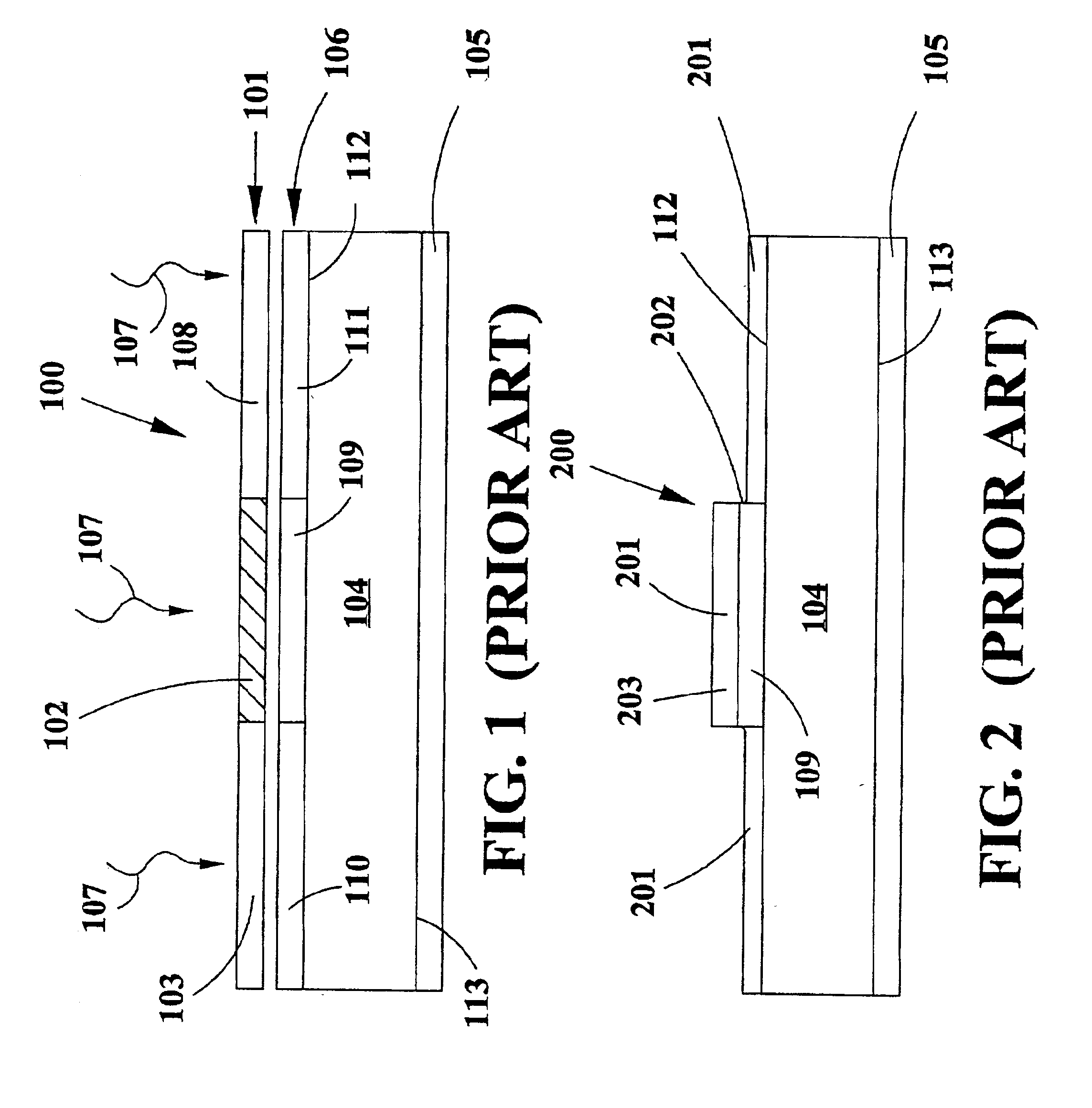
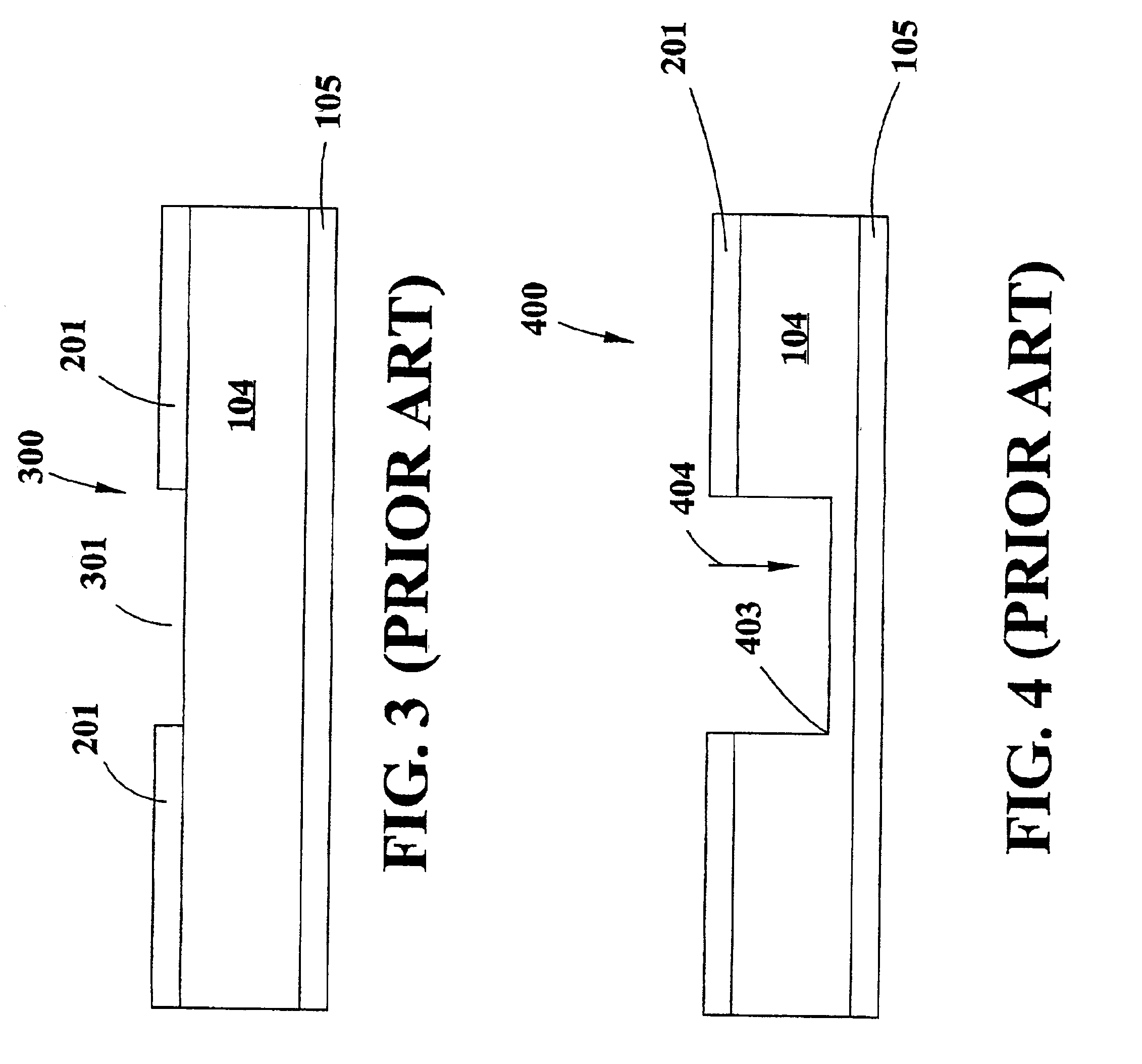
FIG. 1 is a prior art schematic illustration of a portion 100 of a wafer 800 with ultraviolet light 107 applied to a mask 101 which is positioned in proximity to photoresist 106 applied to the back side 112 of a 3C-SiC, 4H-SiC or 6H-SiC wafer 800. The front side 113 of the portion 100 of a wafer 800 has an n-type epilayer 105 on the front side 113 thereof. Reference numeral 113 indicates the p-n junction between the n-type SiC epilayer and the p-type SiC substrate. FIG. 8 is an enlarged view of an entire SiC wafer 800 schematically illustrating a grid system of approximately 500 areas where approximately 500 sensors, for example, can be manufactured.

Mask 101 can contact photoresist 106 or it can be in proximity to the photoresist 106. Mask 101 includes transparent portions 103 and 108 as well as a circular opaque portion 102. The SiC substrate 104 and the n-type SiC epilayer 105 may be any of the 3C-SiC, 4H-SiC or 6H-SiC polytypes. Ultraviolet light imidizes portions 110 and 111 of ...


PUM

PropertyMeasurementUnit
Massaaaaaaaaaa

Abstract

A method of bulk manufacturing SiC sensors is disclosed and claimed. Materials other than SiC may be used as the substrate material. Sensors requiring that the SiC substrate be pierced are also disclosed and claimed. A process flow reversal is employed whereby the metallization is applied first before the recesses are etched into or through the wafer. Aluminum is deposited on the entire planar surface of the metallization. Photoresist is spun onto the substantially planar surface of the Aluminum which is subsequently masked (and developed and removed). Unwanted Aluminum is etched with aqueous TMAH and subsequently the metallization is dry etched. Photoresist is spun onto the still substantially planar surface of Aluminum and oxide and then masked (and developed and removed) leaving the unimidized photoresist behind. Next, ITO is applied over the still substantially planar surface of Aluminum, oxide and unimidized photoresist. Unimidized and exposed photoresist and ITO directly above it are removed with Acetone. Next, deep reactive ion etching attacks exposed oxide not protected by ITO. Finally, hot phosphoric acid removes the Al and ITO enabling wires to connect with the metallization. The back side of the SiC wafer may be also be etched.

Description

ORIGIN OF THE INVENTIONThe invention described herein was made by an employee of the United States Government, and may be manufactured and used by the government for government purposes without the payment of any royalties therein and therefor.This invention is in the field of micro electromechanical devices or related materials.Strain gages have been bonded on metal diaphragms to produce pressure sensors or accelerometers. Because these transducers are made of materials with dissimilar properties, they suffer from coefficient of thermal expansion (CTE) mismatch, which leads to fatigue and early failure. In addition the production process is time consuming since each strain gage must be placed on the diaphragm one at a time.I am a named inventor of U.S. Pat. No. 5,637,905 to Carr et al. and it discloses a high temperature pressure and displacement microsensor made from a Si substrate. A first coil structure is positioned within a recess in the Si and a pressure diaphragm is glass bo...

Claims


Application Information

Patent Timeline
IPC IPC(8): B81B7/00B81C1/00
CPCB81C1/00182B81B2201/0235B81C2201/0133G01P2015/084
Inventor OKOJIE, ROBERT S.
Owner NASA
Why Eureka
Try Eureka