
Eureka
For R&D, Eureka makes reading and utilizing patents & technical documents easy.
Eureka AIR
Designed for self-driven R&D workflows. Generate viable solutions, solve complex R&D challenges, empower your innovation with AI.

Eureka Materials
Designed for material experts only. Revolutionize your material R&D, from search, analyze, to developing new materials.

TechResearch
Generate reliable direction feasibility study reports for your R&D in just a few steps.

TechSeek
Discover and master advanced knowledge NOW. Basics, ideas, possibilities, all at once.

TechMind
As an expert in R&D Theories, TechMind can generates customized viable solutions instantly.

TechRisk
Analyze your overall solution with one click, know your potential R&D risks in advance.

TechMonitor
Get weekly tech updates, stay abreast of the latest tech innovations and key insights.
Optical information recording medium having ultraviolet-curing resin and adhesive layers and method of manufacturing same
- Summary
- Abstract
- Description
- Claims
- Application Information
AI Technical Summary
Benefits of technology
Problems solved by technology
Method used
Image

Examples
first embodiment
(First Embodiment)
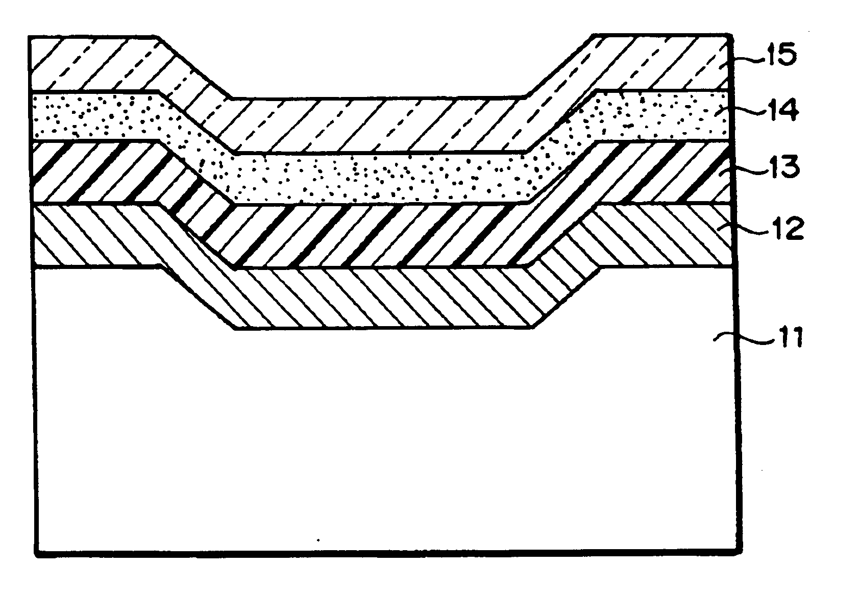
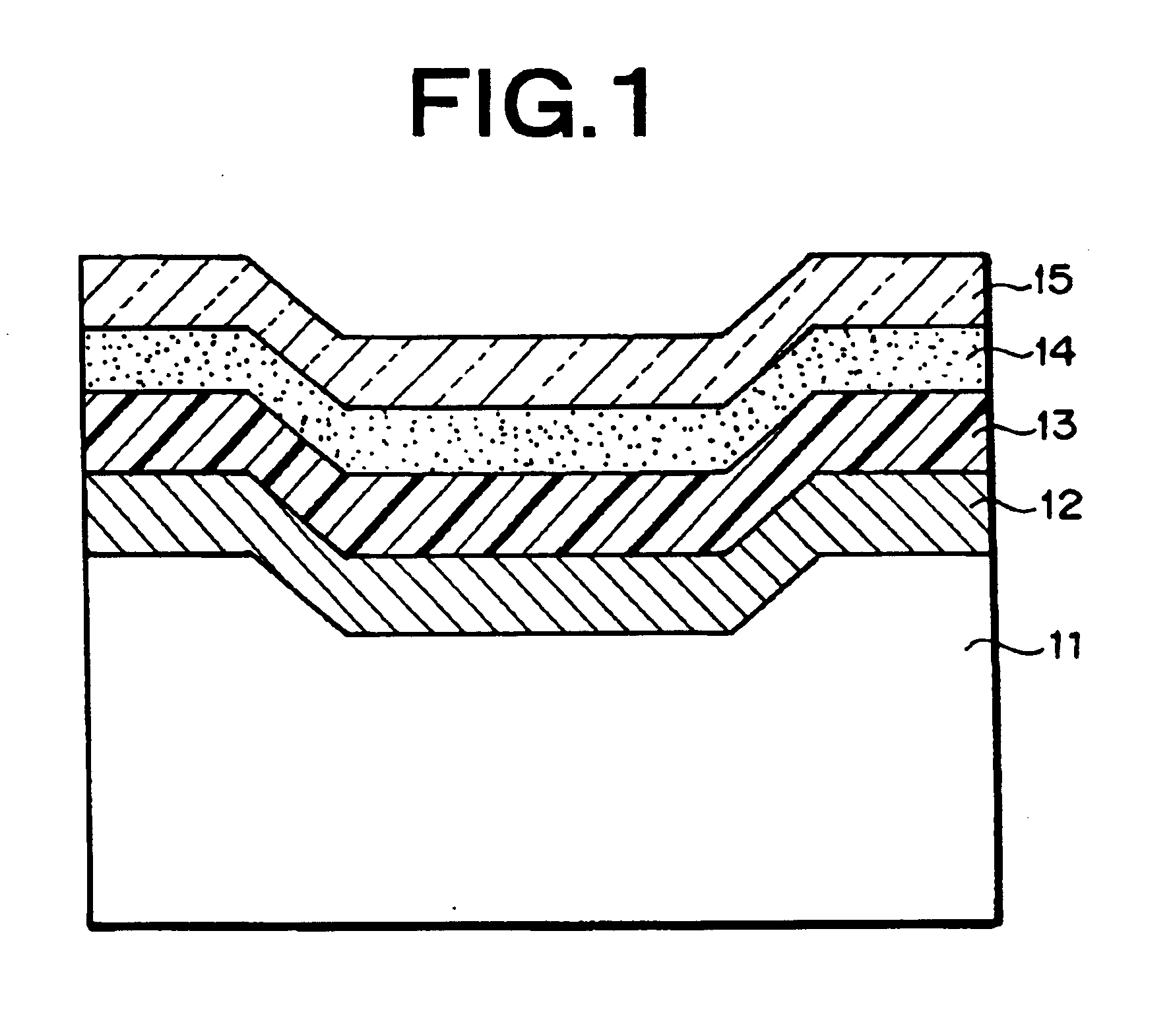
A substrate of polycarbonate having a thickness of 1.2 mm was used, and an Al—Cr reflection layer of 100 nm, a ZnS—SiO2 protection layer of 20 nm, a Ge2Sb2Te5 recording layer of 13 nm and a ZnS—SiO2 protection layer of 50 nm are successively laminated by sputtering. Thereafter, an ultraviolet-curing resin layer of 5 μm in thickness was formed by spin coating, and ultraviolet rays were irradiated to the ultraviolet-curing rein layer to cure the ultraviolet-curing resin layer. Thereafter, a polycarbonate film of 100 μm in thickness was attached to the cured ultraviolet-curing resin layer through an adhesive layer (pressure-sensitive adhesive sheet) of 30 μm in thickness. A guide groove was formed on the substrate so as to have a pitch of 0.6 μm and a depth of 40 nm. The transmittance of the ultraviolet-curing resin layer at the wavelength of 400 nm was equal to about 85%, and the hardness thereof was equal to H.
A semiconductor laser beam was irradiated to the disk wh...
second embodiment
(Second Embodiment)
A substrate of polycarbonate having a thickness of 1.2 mm was used, and an Al-Ti reflection layer of 100 nm, a ZnS—SiO2 protection layer of 15 nm, a Ge2Sb2Te5 recording layer of 12 nm and a ZnS—SiO2 protection layer of 60 nm are successively laminated by sputtering. Thereafter, an ultraviolet-curing resin layer was formed by spin coating, and ultraviolet rays were irradiated to the ultraviolet-curing rein layer to cure the ultraviolet-curing resin layer. Thereafter, a polycarbonate film of 100 μm in thickness was attached to the cured ultraviolet-curing resin layer through an adhesive layer (pressure-sensitive adhesive sheet) of 30 μm in thickness. A guide groove was formed on the substrate so as to have a pitch of 0.6 μm and a depth of 40 nm. The hardness of the ultraviolet-curing resin layer was equal to 2H.
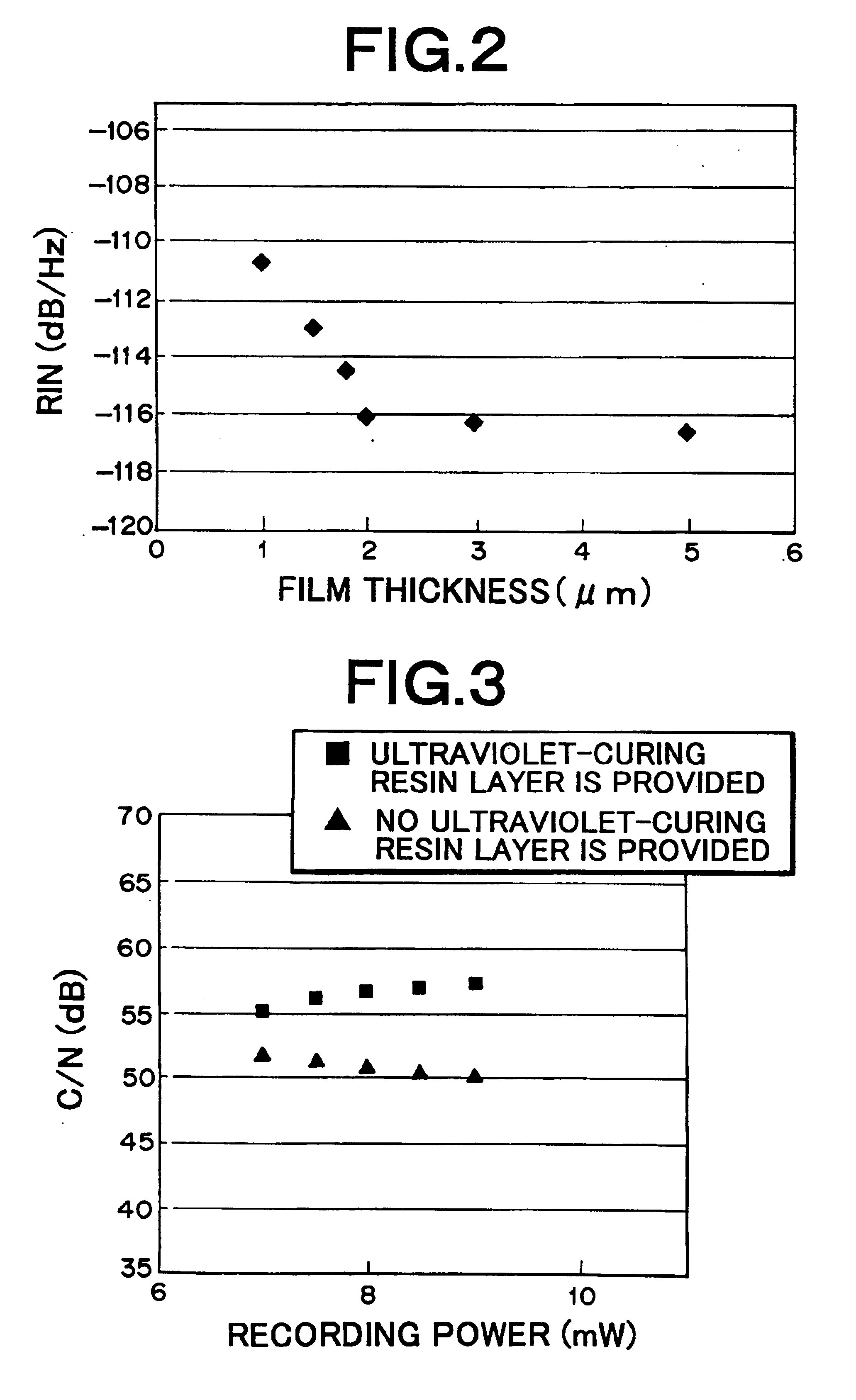
Disks were formed while the film thickness of the ultraviolet-curing resin was varied by changing the condition (rotational number) of the spin coating, and ...
third embodiment
(Third Embodiment)
A substrate of polycarbonate having a thickness of 1.2 mm was used, and a dye-based recording layer and an Al—Ti reflection layer were laminated in this order. Thereafter, an ultraviolet-curing resin layer of 5 μm in thickness was formed by spin coating, and ultraviolet rays were irradiated to the ultraviolet-curing rein layer to cure the ultraviolet-curing resin layer. Thereafter, a polycarbonate film of 100 μm in thickness was attached to the cured ultraviolet-curing resin layer through an adhesive layer (pressure-sensitive adhesive sheet) of 30 μm in thickness. A guide groove was formed on the substrate so as to have a pitch of 0.8 μm and a depth of 40 nm. A signal having a recording frequency of 2 MHz, duty=50% was recorded by using an optical head having 650 nm in wavelength and an objective lens of NA=0.8 while the disk was rotated at a linear velocity of 5 m / s, and C / N (Carrier to Noise Ratio) was measured. For comparison, a light-transmissible film serving ...
PUM
 Abstract
Description
Claims
Application Information
 - R&D Engineer
- R&D Manager
- IP Professional
- Industry Leading Data Capabilities
- Powerful AI technology
- Patent DNA Extraction
Browse by: Latest US Patents, China's latest patents, Technical Efficacy Thesaurus, Application Domain, Technology Topic, Popular Technical Reports.
© 2024 PatSnap. All rights reserved.Legal|Privacy policy|Modern Slavery Act Transparency Statement|Sitemap|About US| Contact US: help@patsnap.com