Vacancy dominated,defect-free silicon

a defect-free silicon and vacancy-dominated technology, applied in the field of semiconductor grade single crystal silicon preparation, can solve the problems of agglomeration intrinsic point defects of rapid increasing importance, affecting the yield potential of materials, and the number of defects in single crystal silicon in the crystal growth chamber

Inactive Publication Date: 2005-01-11
SUNEDISON SEMICON LIMITED UEN201334164H
View PDF15 Cites 7 Cited by
  • Summary
  • Abstract
  • Description
  • Claims
  • Application Information

AI Technical Summary

Benefits of technology

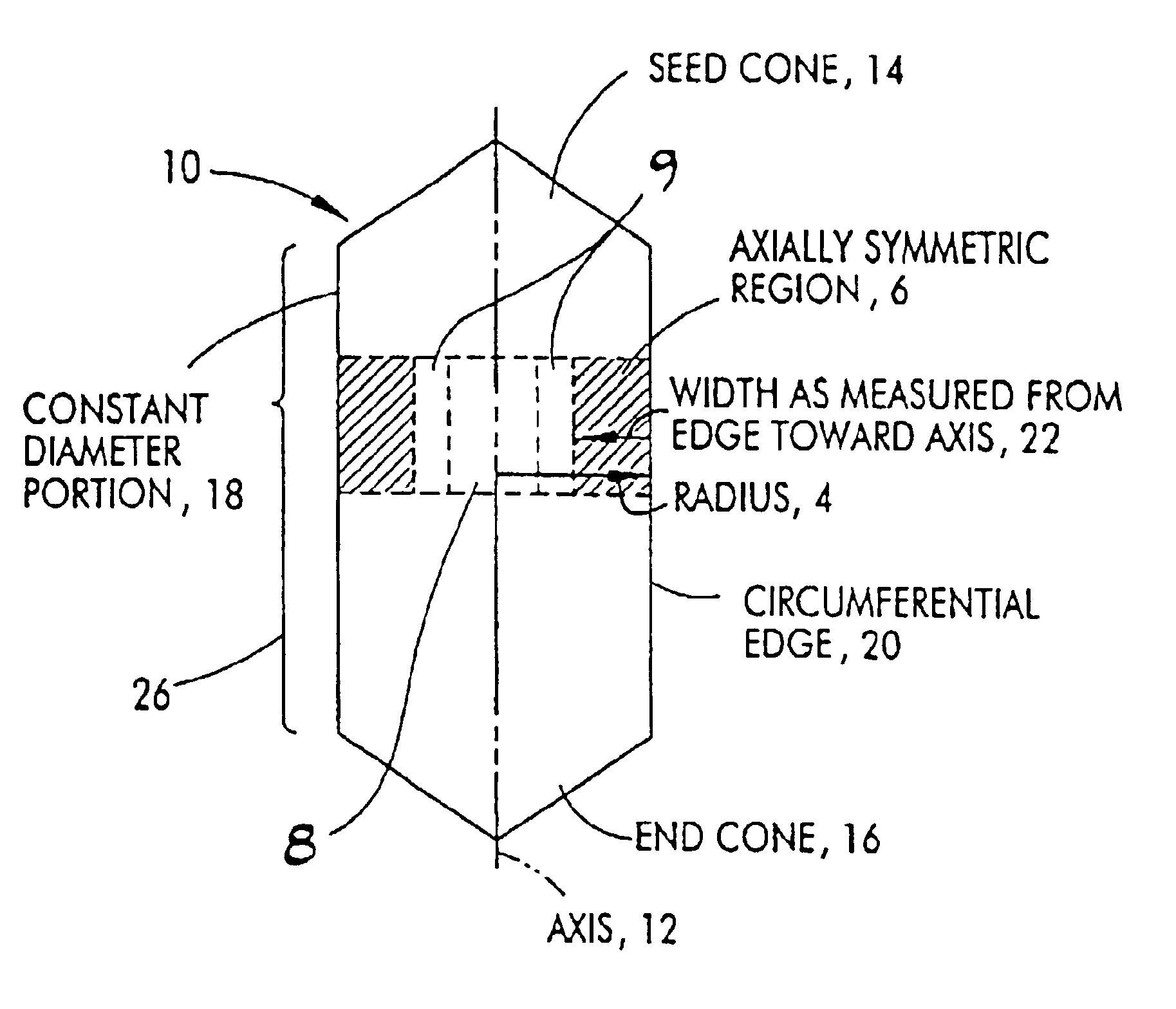
Among the objects of the present invention, therefore, is the provision of single crystal silicon in ingot or wafer form having an axially symmetric region of substantial radial width which is substantially free of defects resulting from an agglomeration of crystal lattice vacancies or silicon self-interstitials; and the provision of a process for preparing a single crystal silicon ingot in which the concentration of vacancies and self-interstitials is controlled in order to prevent an agglomeration of intrinsic point defects in an axially symmetric segment of a constant diameter portion of the ingot, as the ingot cools from the solidification temperature.

Problems solved by technology

In recent years, it has been recognized that a number of defects in single crystal silicon form in the crystal growth chamber as the crystal cools after solidification.
Agglomerated intrinsic point defects in silicon can severely impact the yield potential of the material in the production of complex and highly integrated circuits.
Such defects are not responsible for gate oxide integrity failures, an important wafer performance criterion, but they are widely recognized to be the cause of other types of device failures usually associated with current leakage problems.
While these values are relatively low, agglomerated intrinsic point defects are of rapidly increasing importance to device manufacturers and, in fact, are now seen as yield-limiting factors in device fabrication processes.
While this approach reduces the number density of agglomerated defects, it does not prevent their formation.
As the requirements imposed by device manufacturers become more and more stringent, the presence of these defects will continue to become more of a problem.
This suggestion, however, is also not satisfactory because such a slow pull rate leads to reduced throughput for each crystal puller.
This high concentration, in turn, leads to the formation of agglomerated self-interstitial defects and all the resulting problems associated with such defects.
Furthermore, such wafer heat treatments are relatively costly, have the potential for introducing metallic impurities into the silicon wafers, and are not universally effective for all types of crystal-related defects.
Epitaxial deposition, however, substantially increases the cost of the wafer.

Method used


Image

  • Vacancy dominated,defect-free silicon
  • Vacancy dominated,defect-free silicon
  • Vacancy dominated,defect-free silicon

Examples


example 1

Optimization Procedure for a Crystal Puller Having a Pre-existing Hot Zone Design

A first 200 mm single crystal silicon ingot was grown under conditions in which the pull rate was ramped linearly from about 0.75 mm / min. to about 0.35 mm / min. over the length of the crystal. FIG. 7 shows the pull rate as a function of crystal length. Taking into account the pre-established axial temperature profile of a growing 200 mm ingot in the-crystal-puller and the pre-established radial variations in the average axial temperature gradient, G0, i.e., the axial temperature gradient at the melt / solid interface, these pull rates were selected to insure that ingot would be vacancy dominated material from the center to the edge at one end of the ingot and interstitial dominated material from the center to the edge of the other end of the ingot. The grown ingot was sliced longitudinally and analyzed to determine where the formation of agglomerated interstitial defects begins.

FIG. 8 is an image produced ...

example 2

Reduction of Radial Variation in G0(r)

FIGS. 10 and 11 illustrate the improvement in quality that can be achieved by reduction of the radial variation in the axial temperature gradient at the melt / solid interface, G0(r). The initial concentration (about 1 cm from the melt / solid interface) of vacancies and interstitials are calculated for two cases with different G0(r): (1) G0(r)=2.65+5×10⁻⁴r2 (K / mm) and (2) G0(r)=2.65+5×10⁻⁵r2 (K / mm). For each case the pull rate was adjusted such that the boundary between vacancy-rich silicon and interstitial-rich silicon is at a radius of 3 cm. The pull rate used for case 1 and 2 were 0.4 and 0.35 mm / min, respectively. From FIG. 11 it is clear that the initial concentration of interstitials in the interstitial-rich portion of the crystal is dramatically reduced as the radial variation in the initial axial temperature gradient is reduced. This leads to an improvement in the quality of the material since it becomes easier to avoid the formation of int...

example 3

Increased Out-diffusion Time for Interstitials

FIGS. 12 and 13 illustrate the improvement in quality that can be achieved by increasing the time for out-diffusion of interstitials The concentration of interstitials is calculated for two cases with differing axial temperature profiles in the crystal, dT / dz. The axial temperature gradient at the melt / solid interface is the same for both cases, so that the initial concentration (about 1 cm from the melt / solid interface) of interstitials is the same for both cases. In this example, the pull rate was adjusted such that the entire crystal is interstitial-rich. The pull rate was the same for both cases, 0.32 mm / min. The longer time for interstitial out-diffusion in case 2 results in an overall reduction of the interstitial concentration. This leads to an improvement in the quality of the material since it becomes easier to avoid the formation of interstitial defect clusters due to supersaturation of interstitials.


PUM

PropertyMeasurementUnit
temperatureaaaaaaaaaa

Abstract

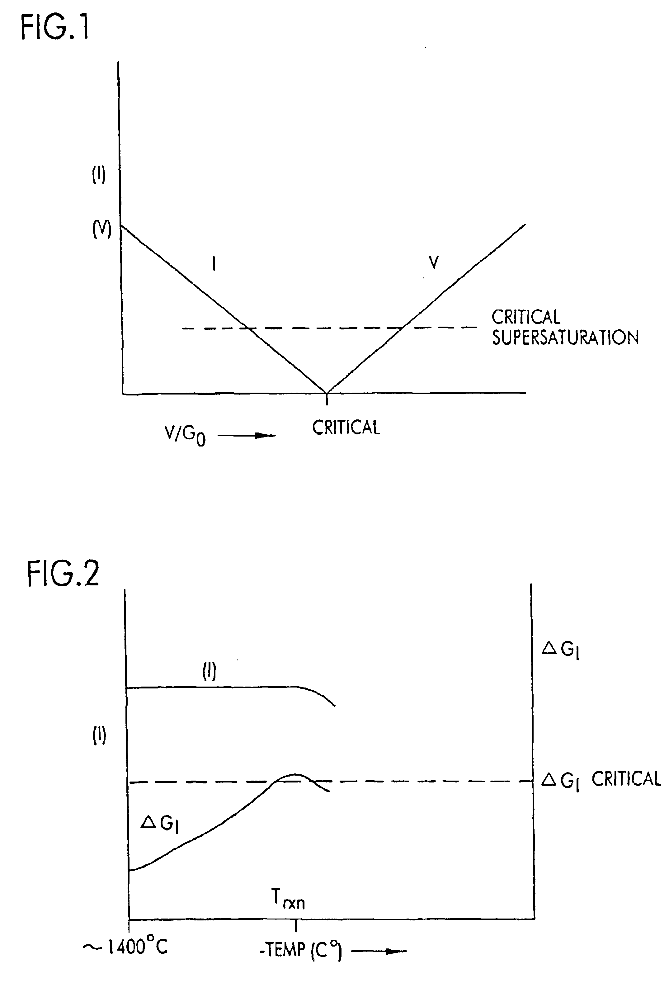
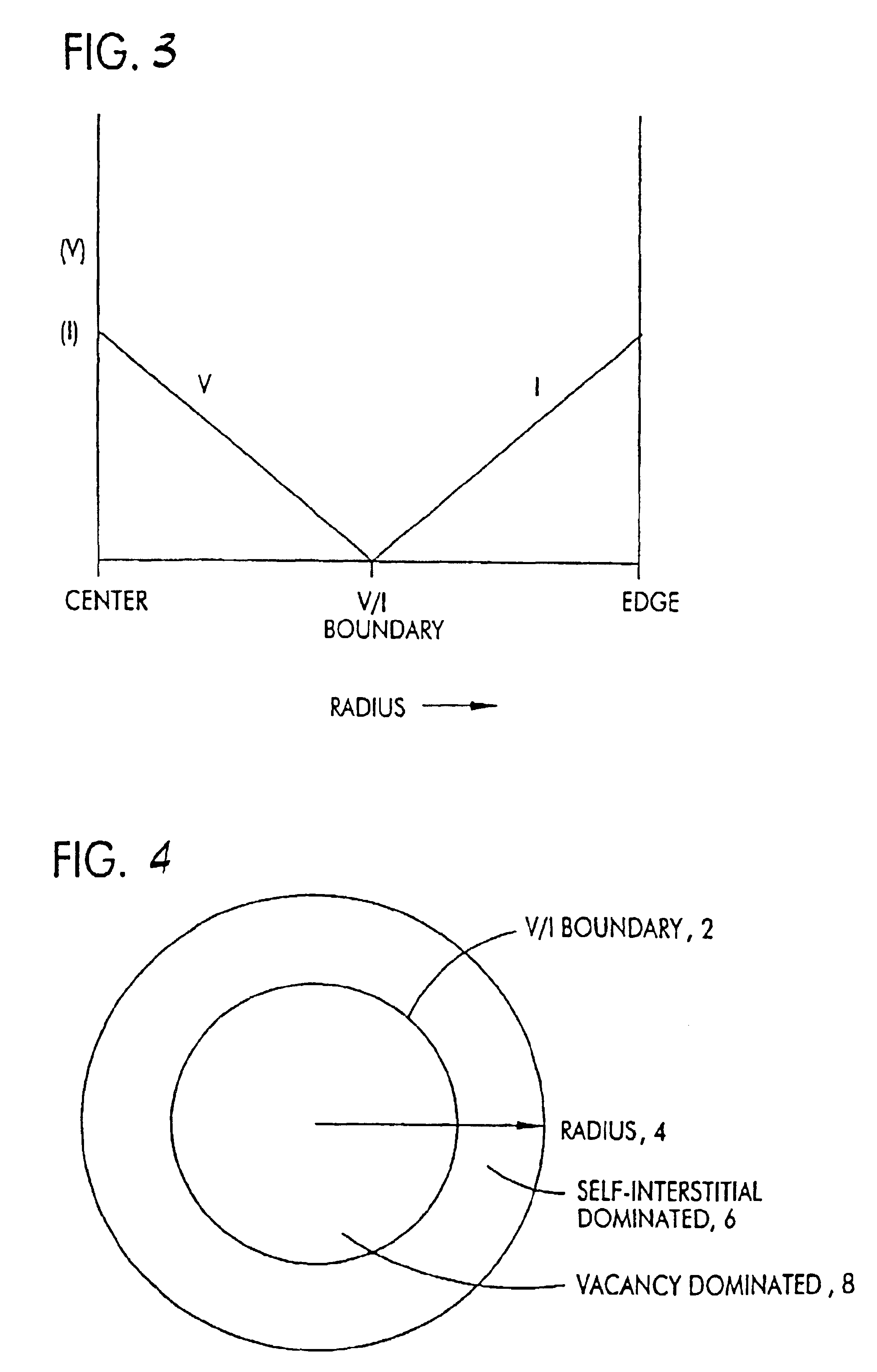
The present invention relates to a process for growing a single crystal silicon. The process including controlling a growth velocity, v, and an average axial temperature gradient, G0, during the growth of the constant diameter portion of the crystal over the temperature range from solidification to a temperature of no less than about 1325° C., to cause the formation of a first axially symmetrical region in which vacancies, upon cooling of the ingot from the solidification temperature, are the predominant intrinsic point defect and which is substantially free of agglomerated intrinsic point defects, wherein the first axially symmetric region has a width of at least about 50% of the radius of the constant diameter portion of the ingot.

Description

BACKGROUND OF THE INVENTIONThe present invention generally relates to the preparation of semiconductor grade single crystal silicon which is used in the manufacture of electronic components. More particularly, the present invention relates to single crystal silicon ingots and wafers having an axially symmetric region of vacancy dominated material which is devoid of agglomerated intrinsic point defects, and a process for the preparation thereof.Single crystal silicon, which is the starting material for most processes for the fabrication of semiconductor electronic components, is commonly prepared by the so-called Czochralski (“Cz”) method. In this method, polycrystalline silicon (“polysilicon”) is charged to a crucible and melted, a seed crystal is brought into contact with the molten silicon and a single crystal is grown by slow extraction. After formation of a neck is complete, the diameter of the crystal is enlarged by decreasing the pulling rate and / or the melt temperature until ...

Claims


Application Information

Patent Timeline
Patent Type & Authority Patents(United States)
IPC IPC(8): C30B33/00C30B15/00H01L21/322H01L21/02C30B15/20C30B15/22C30B29/06H01L29/12
CPCC30B15/00C30B15/20C30B15/203C30B15/206C30B29/06C30B33/00H01L21/3225C30B15/22Y10T428/12528C30B33/02
Inventor FALSTER, ROBERT A.HOLZER, JOSEPH C.MARKGRAF, STEVE A.MUTTI, PAOLOMCQUAID, SEAMUS A.JOHNSON, BAYARD K.
Owner SUNEDISON SEMICON LIMITED UEN201334164H
Why Eureka
Try Eureka