
Non-invasive electrical measurement of semiconductor wafers

Inactive Publication Date: 2005-01-11
SEMICON PHYSICS LAB
View PDF16 Cites 32 Cited by
  • Summary
  • Abstract
  • Description
  • Claims
  • Application Information

AI Technical Summary

Benefits of technology

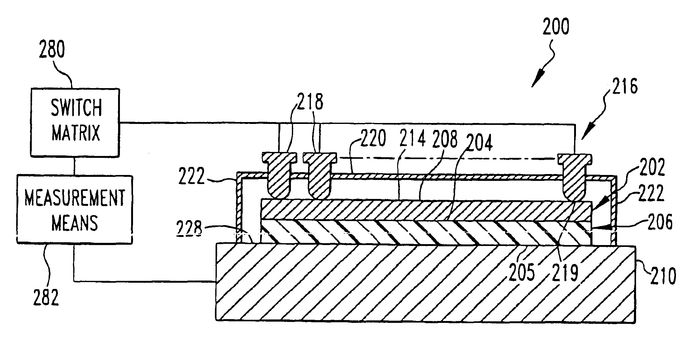
The multi-probe assembly allows for the simultaneous application of many elastic probes to a dielectric or semiconductor surface. Consequently, the semiconductor wafer surface can be mapped without the need for lateral movement between the semiconductor wafer surface and a probe.

Problems solved by technology

In other words, these gates become permanent gates on the semiconductor wafer, thereby making the semiconductor unfit for normal use.
Fabrication of the metal or polysilicon gates is time-consuming and costly.
Problems may arise utilizing the Lederman mercury probe in that mercury may react chemically with the materials of the wafer under study.
Mercury also poses a significant safety problem in its use and mercury sublimes at elevated temperatures when accelerated temperature testing of the semiconductor wafer is desired.
Thus, a mercury probe has limited application.
The relatively small planar contact area between the uniformly flat tip of the probe and the outer surface of the dielectric layer on the wafer resulted in a poor capacitance signal-to-noise ratio when applied to these relatively thick oxides.
A problem with utilizing the probe disclosed in the Hillard patent for performing CV measurements is the need to grind the tip uniformly flat.
Another problem is the need to establish a planar contact between the uniformly flat tip and the outer surface of the dielectric layer of the wafer.
The use of a uniformly flat tip to form a planar contact with the outer surface of the dielectric layer is particularly a problem with today's thin oxide layers since a lack of perfect parallelism between the uniformly flat tip and the outer surface of the dielectric layer may result in an edge surrounding the uniformly flat tip damaging the oxide layer.
One problem with forming test structures in scribe lines of product semiconductor wafers includes the additional processing steps necessary to form these test structures.
Another problem is the need to test these test structures apart from the testing of the integrated circuits formed on the product semiconductor wafer.

Method used


Image

  • Non-invasive electrical measurement of semiconductor wafers
  • Non-invasive electrical measurement of semiconductor wafers
  • Non-invasive electrical measurement of semiconductor wafers

Examples


Embodiment Construction

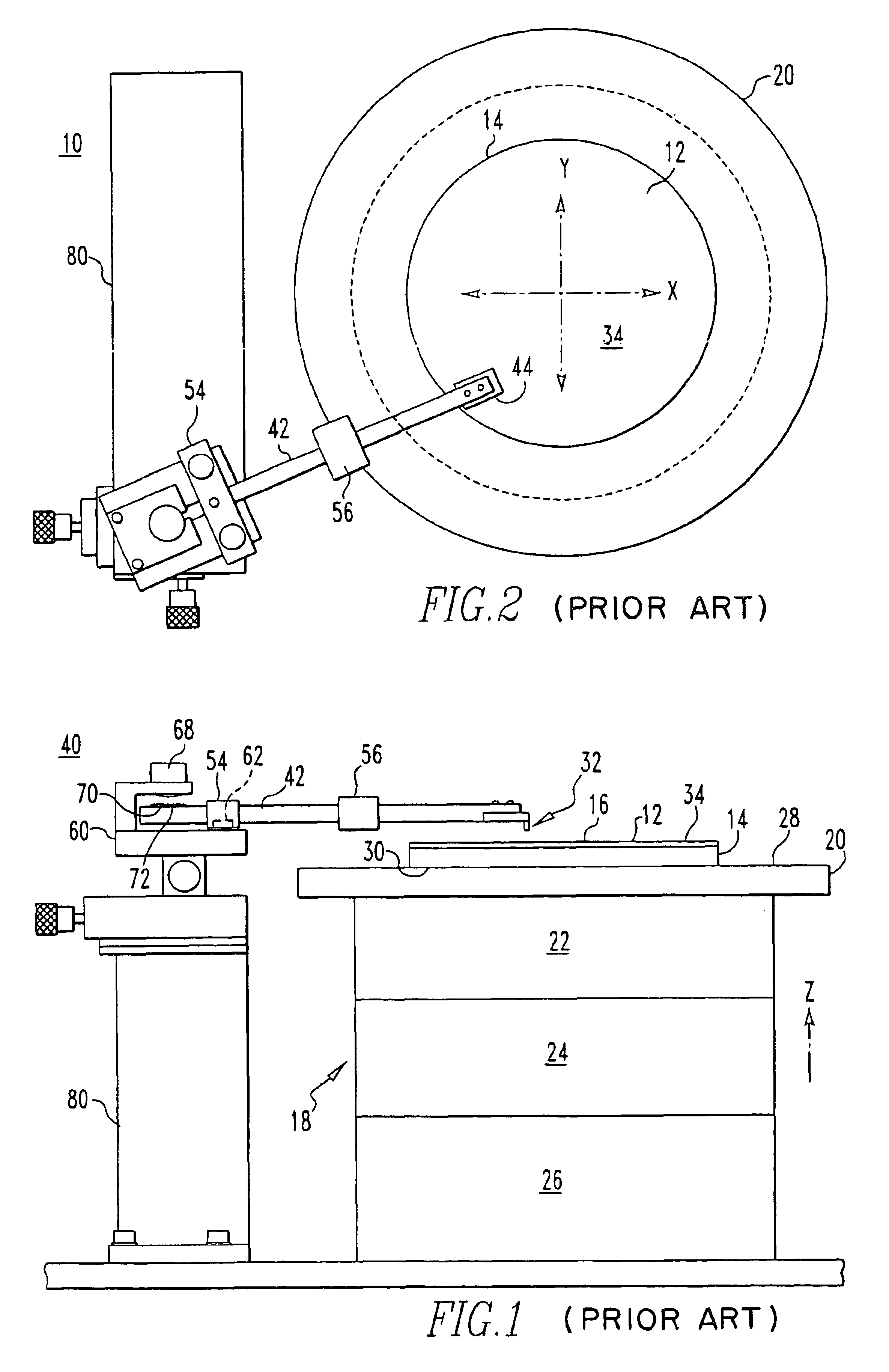
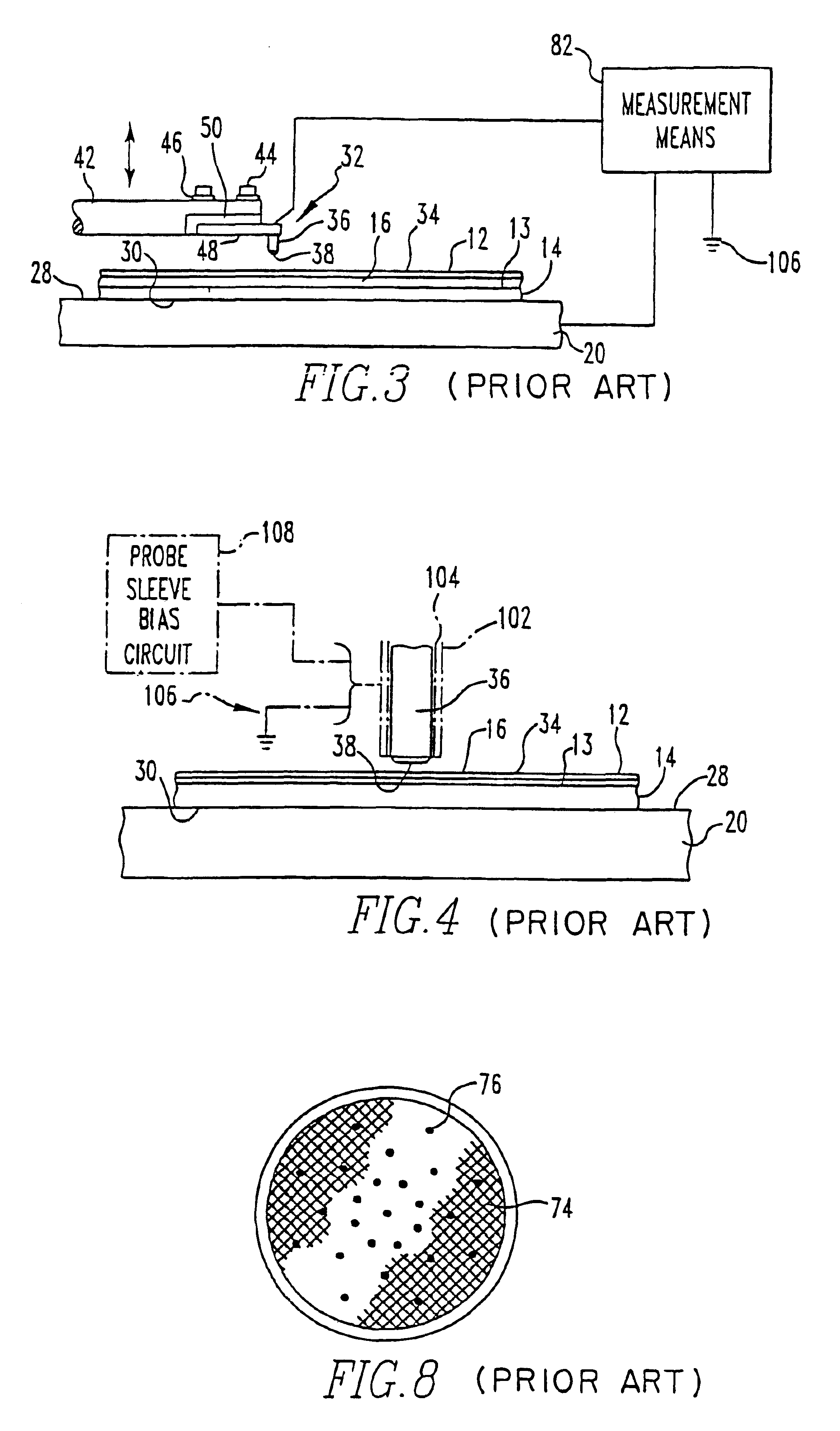
Referring to FIGS. 1-3, an apparatus 10 for measuring electrical properties of a dielectric 12 on a front surface 13 of a semiconductor wafer 14 or in a region 16 of the semiconducting material adjacent the front surface 13 of the semiconductor wafer 14 includes a movable stage assembly 18. Movable stage assembly 18 includes a vacuum chuck 20 which holds semiconductor wafer 14 by means of vacuum. Preferably, movable stage assembly 18 includes a first or rotary stage 22 for rotating semiconductor wafer 14 in an X-Y plane, a second or Z stage 24 for adjusting the vertical position of semiconductor wafer 14, and a third or X / X-Y stage 26 for moving semiconductor wafer 14 in an X or X-Y direction, respectively.

Apparatus 10 includes a first electrical contact 32 for contacting an upper or front surface 34 of dielectric 12. First electrical contact 32 includes a conductive probe 36 preferably having a cylindrically-shaped stainless steel shank. Chuck 20 includes an upper or front surface ...


PUM


Abstract

A multi-probe assembly includes a chuck assembly configured to receive a back or front surface of a semiconductor wafer. A multi-probe holder has a plurality of probes each having an elastically deformable conductive tip movable into contact with a front surface of a dielectric or a front surface of a semiconducting material. A means applies an electrical stimulus to each tip, measures a response to the electrical stimulus, and determines at least one electrical property of the dielectric and / or the semiconducting material. A method for measuring at least one electrical property applies a probe (or plurality of probes) having an elastically deformable conductive tip to a scribe line(s). An electrical stimulus is applied to the probe or one of the probes with the remaining probes grounded. A response to the electrical stimulus is measured and at least one electrical property of the semiconductor wafer is determined from the response.

Description

BACKGROUND OF THE INVENTION1. Field of the InventionThis invention relates generally to an apparatus and method for measuring electrical properties of a semiconductor wafer.2. Description of Related ArtThe determination of electrical properties of a dielectric on a semiconductor wafer and / or a carrier density profile within the semiconductor wafer is a critical factor in the production of such wafers. Measurements based on capacitance-voltage (CV) or capacitance-time (Ct) techniques, such as measurements of dielectric thickness, oxide charge, threshold voltage, implant dose and carrier profile; measurements based on conductance-voltage (GV) techniques, such as measurement of interface state density; and measurements based on current-voltage (IV) techniques, such as dielectric leakage current and breakdown voltage, are typically accomplished by first fabricating metal or doped polysilicon gates on the dielectric. These gates become part of a metal oxide semiconductor (MOS) structure ...

Claims


Application Information

Patent Timeline
IPC IPC(8): G01R31/28G01R31/312G01R1/06H01L21/66
CPCG01R31/2886G01R31/312H01L22/14H01L2924/0002H01L2924/00
Inventor HOWLAND, WILLIAM H.
Owner SEMICON PHYSICS LAB
Learn More