Thin film magnetic memory device executing self-reference type data read

a magnetic memory device and self-reference technology, applied in semiconductor devices, digital storage, instruments, etc., can solve the problems of deteriorating data read accuracy, difficult to accurately set the reference current level, and possible large changes in pass current in response to even a small fluctuation in voltage, and achieve high-rate data read operation

Inactive Publication Date: 2005-01-11
RENESAS ELECTRONICS CORP
View PDF4 Cites 59 Cited by
  • Summary
  • Abstract
  • Description
  • Claims
  • Application Information

AI Technical Summary

Benefits of technology

[0044]The thin film magnetic memory device generates the read data on the basis of the difference between the voltage of the data line of the selected memory cell before the application of the data write magnetic field and the voltage of the data line of the selected memory cell after the application of a predetermined data write magnetic field. The data read before the application, the application of the data write magnetic field, and the data read after the application, are continuously executed. So-called read modify write for continuously executing read and write when executing the data read by self-reference cell method which does not employ a reference cell, is used. Therefore, it is possible to execute a high data read operation.
[0046]The thin film magnetic memory device executes the so-called self-reference read operation using the memory cell consisting only of a magneto-resistance element without an access element. This simplifies the structure of the memory cell, making it possible to reduce the area of the memory array.
[0048]According to the thin film magnetic memory device, the memory cell consists only of a magneto-resistance element without an access element. Using the fact that the electric resistance of the selected memory cell is changed with a polarity according to the stored data by applying the bias magnetic field along the hard axis, the self-reference data read for accessing only the selected memory cell can be executed without executing forced data write and data read and the rewriting of the stored data to the selected memory cell. It is thereby possible to execute a high rate data read operation.

Problems solved by technology

However, the reference cell using access diode DY operates in a built potential voltage region at 0.5 V. As a result, the pass current may possibly greatly change in response to even a small fluctuation in voltage.
For this reason, it is difficult to accurately set the level of the reference current generated by the reference cell and there is a fear of the deterioration of data read accuracy due to the fluctuation in reference current.
However, if tunnel thickness accuracy is set strict in manufacturing process, it is considered that manufacturing cost hike accompanying the deterioration of manufacturing yield may occur.

Method used


Image

  • Thin film magnetic memory device executing self-reference type data read
  • Thin film magnetic memory device executing self-reference type data read
  • Thin film magnetic memory device executing self-reference type data read

Examples


second embodiment

[0065]FIG. 16 is a block diagram of a circuit group for executing a data read operation and a data write operation according to the present invention;

[0066]FIG. 17 is a timing chart for the data write operation in the second embodiment;

[0067]FIG. 18 is a timing chart for the data read operation in the second embodiment;

[0068]FIG. 19 is a block diagram of a circuit group for executing a data read operation and a data write operation according to a modification of the second embodiment of the present invention;

[0069]FIG. 20 is a timing chart for the data read operation in the modification of the second embodiment;

[0070]FIG. 21 is a schematic diagram showing the configuration of a memory cell having a tunnel junction;

[0071]FIG. 22 is a conceptual view for describing a data write operation to an MTJ memory cell;

[0072]FIG. 23 is conceptual view showing the relationship between a data write current and the magnetic direction of a tunnel magneto-resistance element during data write;

[0073]F...

first embodiment

[0078

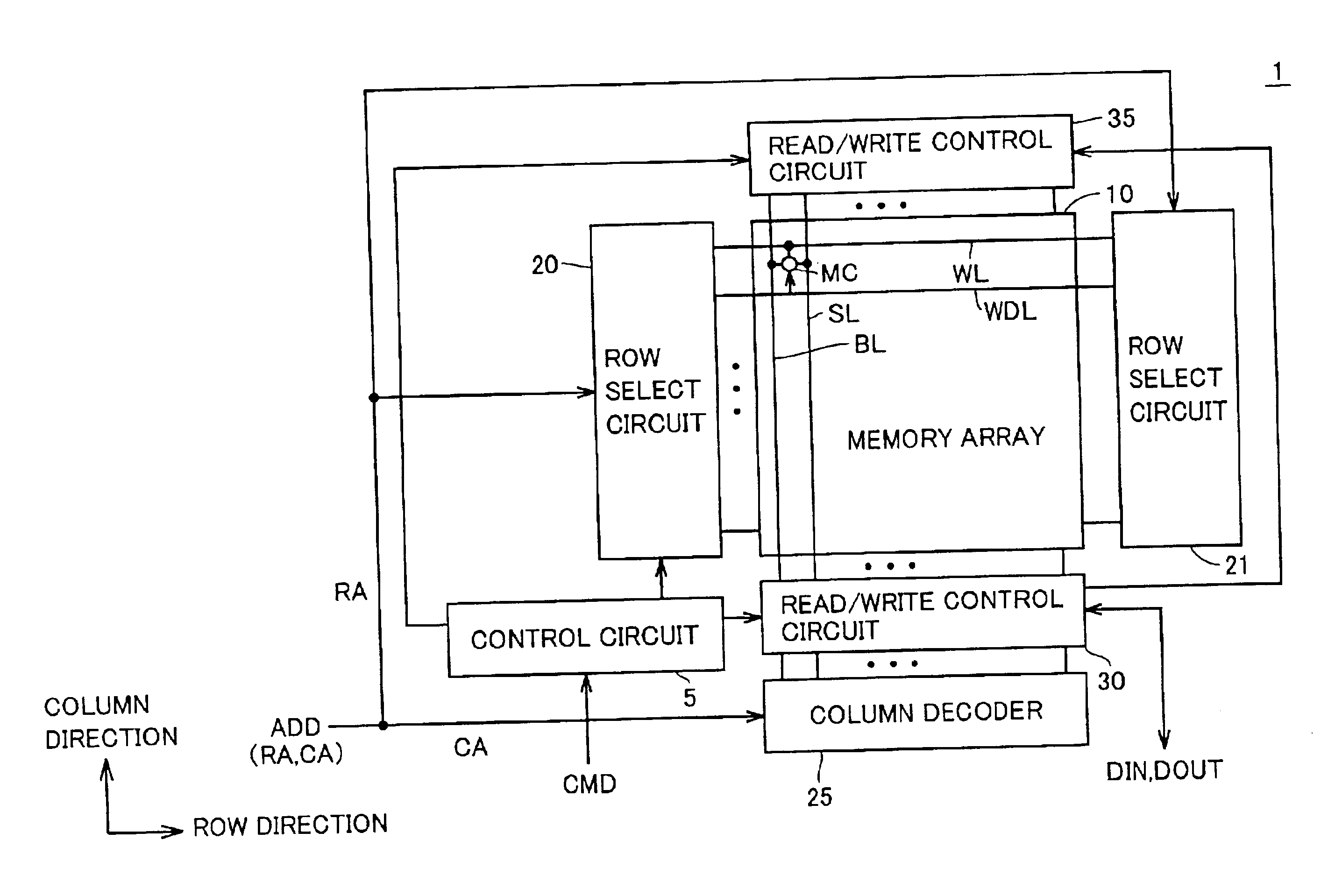
[0079]Referring to FIG. 1, an MRAM device 1 according to the first embodiment of the present invention randomly accesses a memory cell in response to an external control signal CMD and an external address signal ADD, and executes writing input data DIN and reading read data DOUT.

[0080]MRAM device 1 includes a control circuit 5 which controls the overall operation of MRAM device 1 in response to control signal CMD, and a memory array 10 which includes a plurality of MTJ memory cells MC arranged in a matrix.

[0081]The row and column of a plurality of tunnel magneto-resistance elements TMR arranged in memory array 10 in a matrix will be also referred to as “memory cell row” and “memory cell column” hereinafter, respectively.

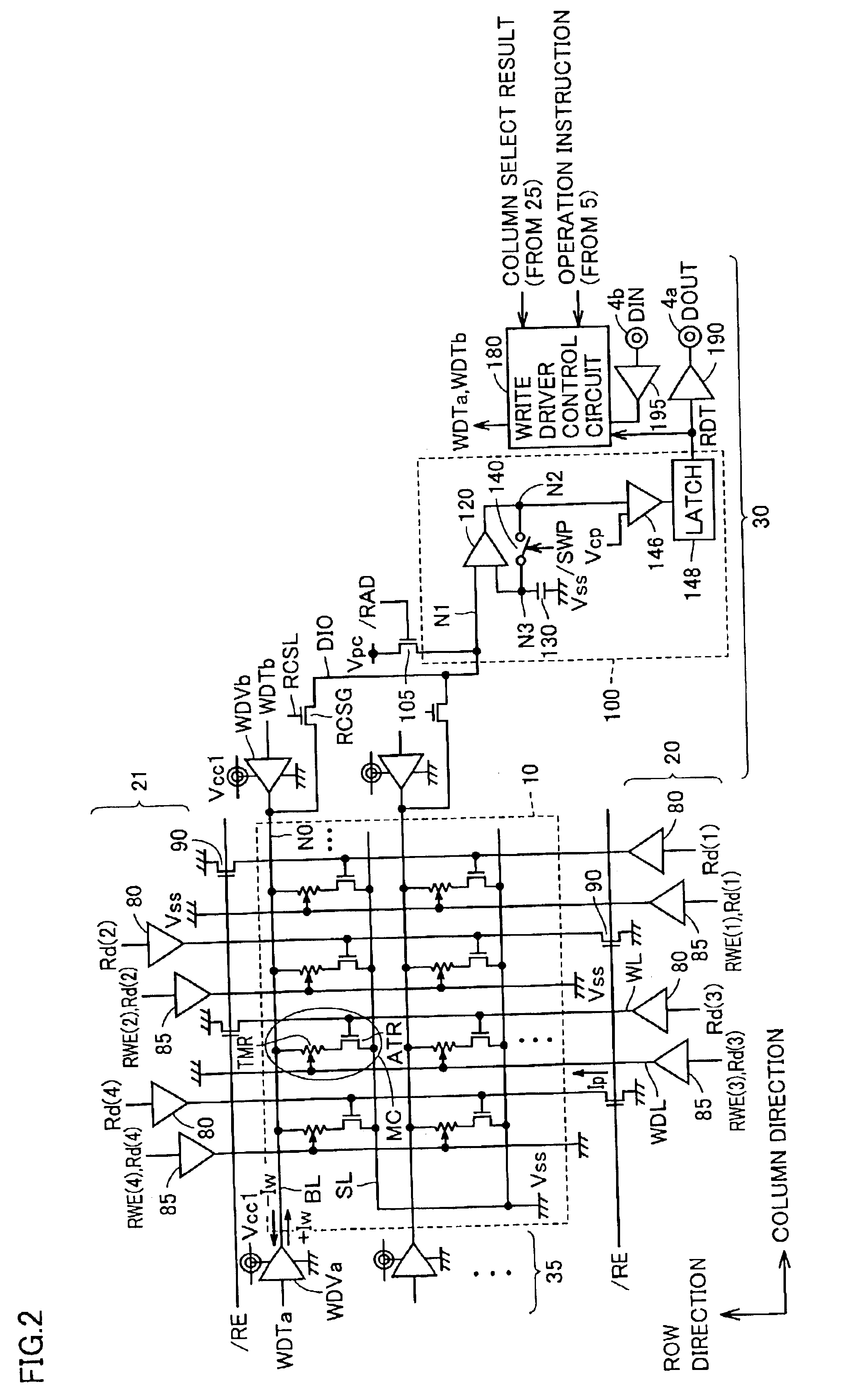
[0082]Since the configuration of tunnel magneto-resistance element TMR and the principle of data storage are the same as those already described with reference to FIGS. 21 to 25, they will not be repeatedly described herein in detail. Each tunnel magneto-resista...


PUM


Abstract

In one data read operation, data read for reading stored data before and after a predetermined data write magnetic field is applied to a selected memory cell, respectively, is executed, and the data read is executed in accordance with comparison of voltage levels corresponding to the data read operations before and after application of the predetermined data write magnetic field. In addition, data read operations before and after the application of a data write magnetic field are executed using read modify write. It is thereby possible to avoid an influence of an offset or the like resulting from manufacturing irregularities in respective circuits forming a data read path, to improve efficiency of the data read operation with accuracy and to execute a high rate data read operation.

Description

BACKGROUND OF THE INVENTION[0002]1. Field of the Invention[0003]The present invention relates to a thin film magnetic memory device, and more particularly to a random access memory including memory cells having magnetic tunnel junctions (MTJ).[0004]2. Description of the Background Art[0005]Attention has been paid to an MRAM (Magnetic Random Access Memory) device as a memory capable of storing data in a nonvolatile manner with low power consumption. MRAM device is a memory which stores nonvolatile data using a plurality of thin film magnetic materials formed on a semiconductor integrated circuit, and which can randomly access the respective thin film magnetic materials.[0006]Recently, it is particularly made public that the performance of MRAM device surprisingly develops by employing thin film magnetic materials utilizing magnetic tunnel junctions as memory cells.[0007]FIG. 21 is a schematic diagram showing the configuration of a memory cell having a tunnel junction (also simply ref...

Claims


Application Information

Patent Timeline
Patent Type & Authority Patents(United States)
IPC IPC(8): G11C11/15G11C11/02H01L21/8246H01L27/105H01L43/08
CPCG11C11/15G11C11/1673
Inventor TANIZAKI, HIROAKIOOISHI, TSUKASAHIDAKA, HIDETO
Owner RENESAS ELECTRONICS CORP
Why Eureka
Try Eureka