Method for preventing low-k dielectric layer cracking in multi-layered dual damascene metallization layers

a dual damascene and dielectric layer technology, applied in the direction of semiconductor/solid-state device manufacturing, basic electric elements, electric apparatus, etc., can solve the problems of difficult interconnection technology, increased rc time constant effect on signal delay, and easy diffusion of copper through silicon dioxide or silicon dioxide based materials, so as to improve crack initiation and propagation resistance

Inactive Publication Date: 2005-01-25
TAIWAN SEMICON MFG CO LTD
View PDF7 Cites 39 Cited by
  • Summary
  • Abstract
  • Description
  • Claims
  • Application Information

AI Technical Summary

Benefits of technology

To achieve the foregoing and other objects, and in accordance with the purposes of the present invention, as embodied and broadly described herein, the present invention provides a method for plasma treatment of anisotropically etched openings to improve a crack initiation and propagation resistance.

Problems solved by technology

As device sizes decrease it has been increasingly difficult to provide interconnection technology that satisfies the requirements of low RC (resistance capacitance) metal interconnect properties, particularly wherein submicron via / contact holes (inter-layer interconnects) and intra-layer interconnects with increasingly high aspect ratios.
As integrated circuits become more complex and feature sizes decrease, the effect of the RC time constant on signal delay becomes greater.
One problem with copper interconnects has been the fact that copper readily diffuses through silicon dioxide or silicon dioxide based materials, a typical IMD material.
The diffusion of copper into the IMD layer reduces both the effectiveness of the electrical interconnect and the electrical insulation properties of the IMD layers.
Another problem is that copper has poor adhesion to silicon dioxide based IMD layers.
The technological difficulties associated with the use of copper have additionally manifested themselves in parallel efforts to reduce the capacitance contribution of the IMD layers to the RC time constant, such reduction being necessary to achieve increased signal transport speeds.
One difficulty is that the reduced strength of low-k materials in combination with thinner layers frequently results in cracking when such materials are subjected to thermal stresses.
Porous low-k materials have a drawback in that the porosity tends to weaken the overall strength and hardness of the material making crack initiation and propagation more likely.
The result is that cracking becomes more likely as the number of device layers increase and the process wafer is subjected to externally induced cycling stresses including thermal heating and cooling.
One particular serious problem that requires a solution is the tendency for copper filled damascene structures that are in upper levels, for example, above about metallization layer 3 to exhibit crack initiation and propagation through low-k IMD layers as a result of thermal cycling stresses.
The problem of cracking is exacerbated in a multiple layer structure where multiple stresses in the various layers may combine to achieve stresses necessary for crack initiation and propagation.
The propagation of cracks through the IMD layer is catastrophic to device functioning and frequently requires the scraping of a process wafer.

Method used


Image

  • Method for preventing low-k dielectric layer cracking in multi-layered dual damascene metallization layers
  • Method for preventing low-k dielectric layer cracking in multi-layered dual damascene metallization layers
  • Method for preventing low-k dielectric layer cracking in multi-layered dual damascene metallization layers

Examples


Embodiment Construction

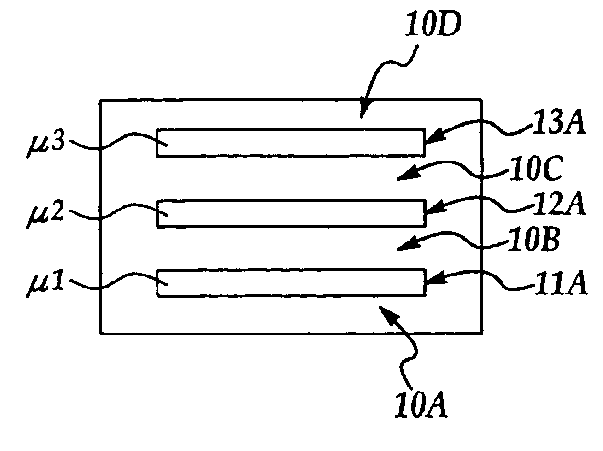
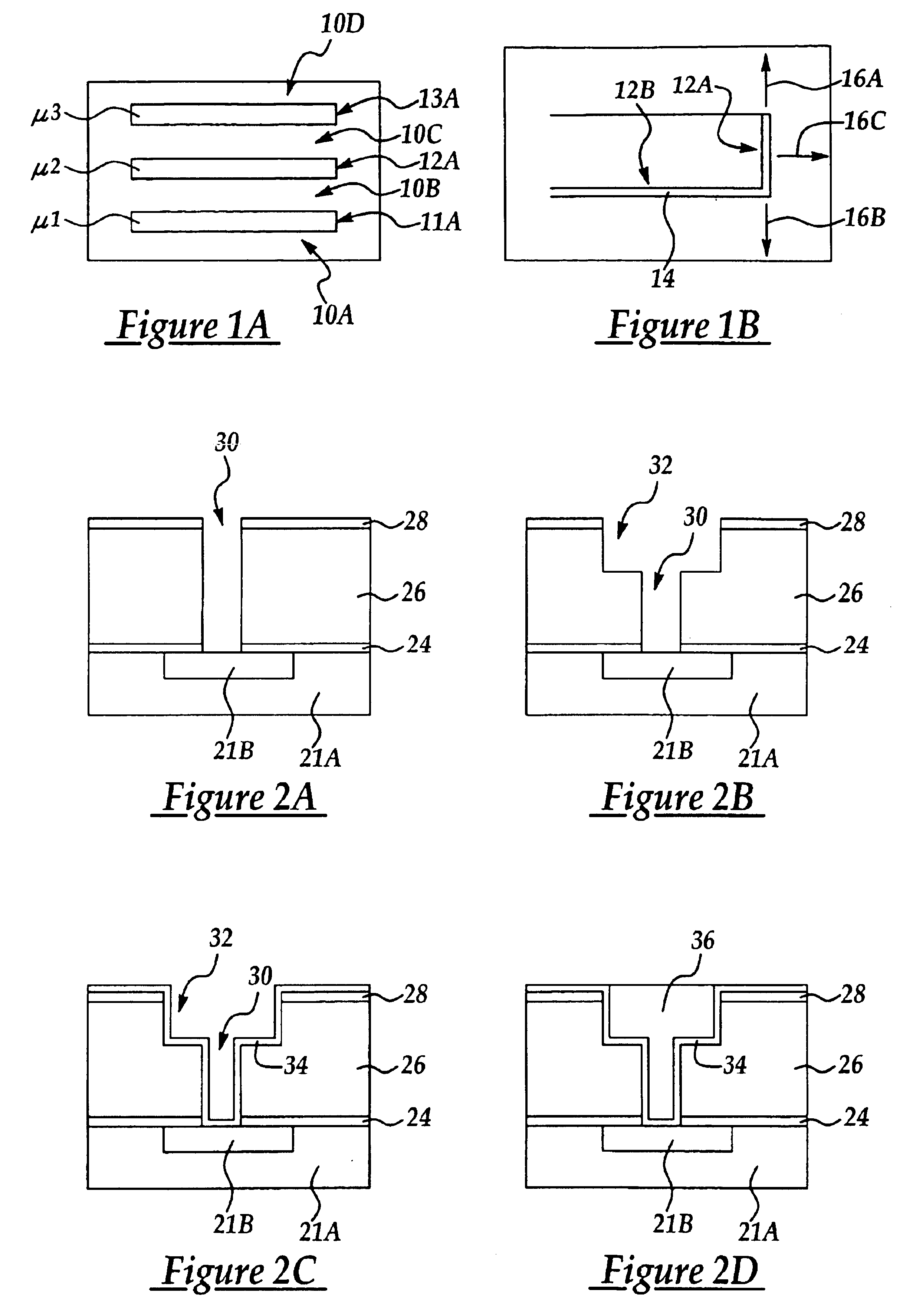
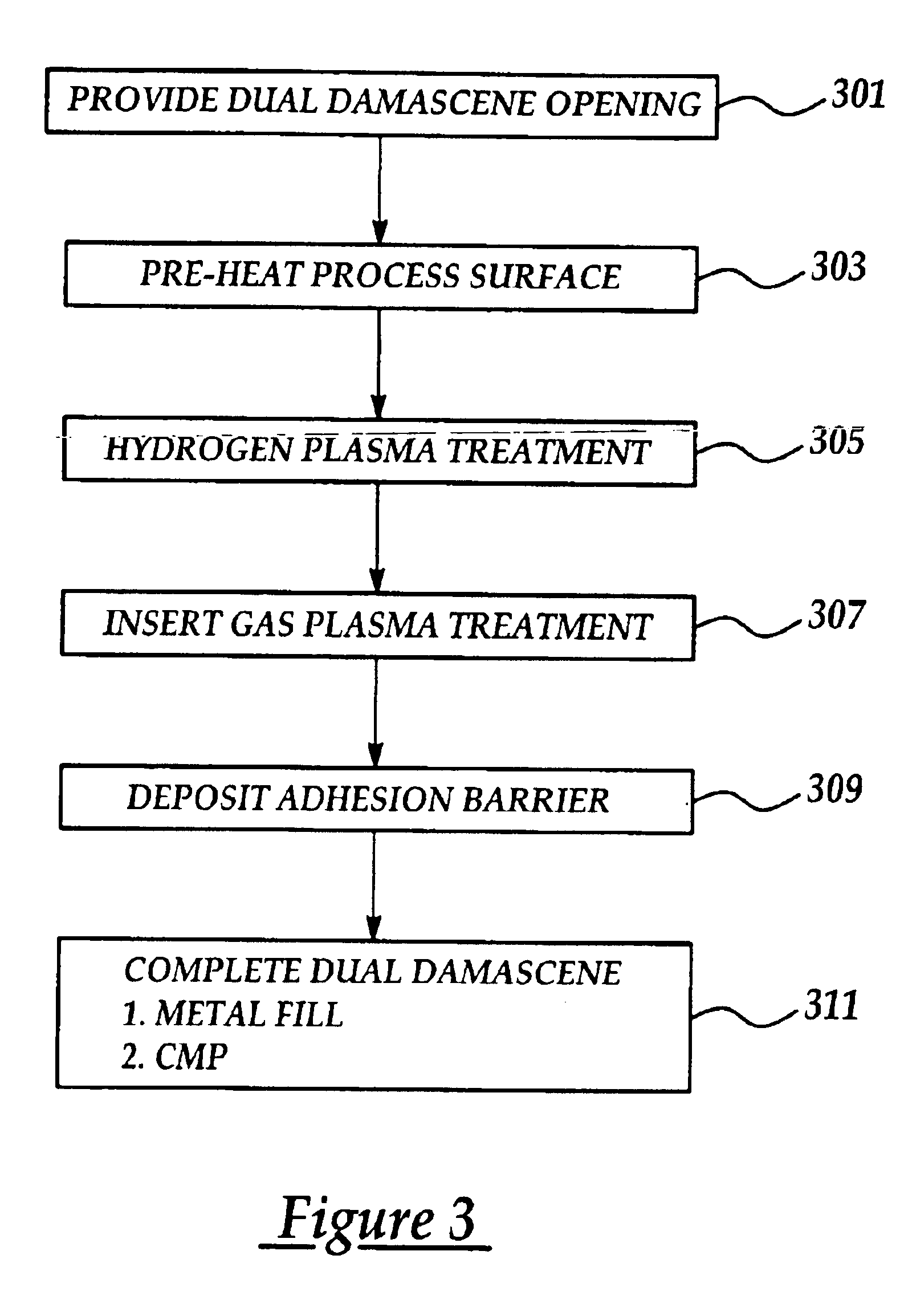
Although the method of the present invention is explained by exemplary reference the formation of a dual damascene structure according to a via-first method of formation in a multi-level semiconductor device it will be appreciated that the method of the present invention is equally applicable to other methods of dual or single damascene structure formation including other metal filled anisotropically etched openings. While the method of the present invention is particularly advantageously implemented with respect to copper filled dual damascene structures, it will be appreciated that the method may be adapted for use with other metals, for example tungsten, aluminum, and copper or alloys thereof in a multi-layered semiconductor device to improve an adhesion / barrier layer adhesion strength thereby preventing stress induced crack initiation and propagation through a dielectric insulating layer. For example, although the method of the present invention is particularly advantageously im...


PUM

PropertyMeasurementUnit
self-bias voltageaaaaaaaaaa
temperatureaaaaaaaaaa
voltageaaaaaaaaaa

Abstract

A method for plasma treatment of anisotropically etched openings to improve a crack initiation and propagation resistance including providing a semiconductor wafer having a process surface including anisotropically etched openings extending at least partially through a dielectric insulating layer; plasma treating in at least one plasma treatment the process surface including the anisotropically etched openings to improve an adhesion of a subsequently deposited refractory metal adhesion / barrier layer thereover; and, blanket depositing at least one refractory metal adhesion / barrier layer to line the anisotropically etched openings.

Description

FIELD OF THE INVENTIONThis invention generally relates to multi-layered semiconductor structures and more particularly to a method for preventing cracking in multi-layered dual damascenes.BACKGROUND OF THE INVENTIONThe escalating requirements for high density and performance associated with ultra large scale integration semiconductor wiring require increasingly sophisticated interconnection technology. As device sizes decrease it has been increasingly difficult to provide interconnection technology that satisfies the requirements of low RC (resistance capacitance) metal interconnect properties, particularly wherein submicron via / contact holes (inter-layer interconnects) and intra-layer interconnects with increasingly high aspect ratios.In the fabrication of semiconductor devices, increased device density requires multiple layers, making necessary the provision of a multi-layered interconnect structure. Such a multi-layered interconnect structure typically includes intra-layer conduc...

Claims


Application Information

Patent Timeline
Patent Type & Authority Patents(United States)
IPC IPC(8): H01L21/02H01L21/30H01L21/70H01L21/768H01L21/311
CPCH01L21/3003H01L21/76843H01L21/76807H01L21/76814H01L21/31116H01L21/31127
Inventor PAN, SHING-CHYANGLIN, KENG-CHUCHIOU, WEN-CHIHJENG, SHWANG-MING
Owner TAIWAN SEMICON MFG CO LTD
Why Eureka
Try Eureka