Well bias voltage control circuit and method

a control circuit and bias voltage technology, applied in the direction of process and machine control, pulse technique, instruments, etc., can solve the problems of leakage current not being compensated, leakage current increasing, power consumption corresponding to leakage current in the power consumption of the circuit increasing, etc., to achieve the ratio of power consumption and leakage current increasing

Inactive Publication Date: 2005-01-25
RENESAS ELECTRONICS CORP
View PDF8 Cites 44 Cited by
  • Summary
  • Abstract
  • Description
  • Claims
  • Application Information

AI Technical Summary

Benefits of technology

When the performance of a transistor varies according to a fabricating process and a difference occurs between a threshold voltage of a PMOS transistor and a threshold voltage of an NMOS transistor, even if the circuit speed is the same, leakage currents of the circuits may differ from each other. This happens for the reason that the leakage current depends on, not the circuit operation speed, but a threshold voltage of a transistor. In the technique, the body bias is controlled to maintain the operation speed, so that the circuit speed can be compensated. However, when the threshold voltage varies, the leakage current cannot be compensated. If decrease in the voltage is further advanced and the threshold voltage of a transistor decreases in future, the variations in the threshold voltage become conspicuous. As a result, the leakage current increases, and the ratio of the power consumption corresponding to the leakage current in the power consumption of the circuit increases. Consequently, compensation of the leakage current is an important technique.
According to the invention, as a well bias control circuit for compensating the threshold voltage difference between a PMOS transistor and an NMOS transistor, in a part of the, region of a main circuit constructed by a CMOS, a control circuit simulating a critical path of the main circuit constructed by the CMOS and including a delay monitor for monitoring a delay in the path is formed in a process of forming the main circuit. The control circuit is provided with a PN Vt balance compensation circuit for compensating an output of the delay monitor in accordance with the threshold voltage difference between the PMOS and NMOS transistors, thereby compensating the circuit speed by monitoring the delay of the path and compensating the threshold voltage difference between the PMOS and NMOS transistors by the PN Vt balance compensation circuit.

Problems solved by technology

However, when the threshold voltage varies, the leakage current cannot be compensated.
As a result, the leakage current increases, and the ratio of the power consumption corresponding to the leakage current in the power consumption of the circuit increases.

Method used


Image

  • Well bias voltage control circuit and method
  • Well bias voltage control circuit and method
  • Well bias voltage control circuit and method

Examples


embodiment i

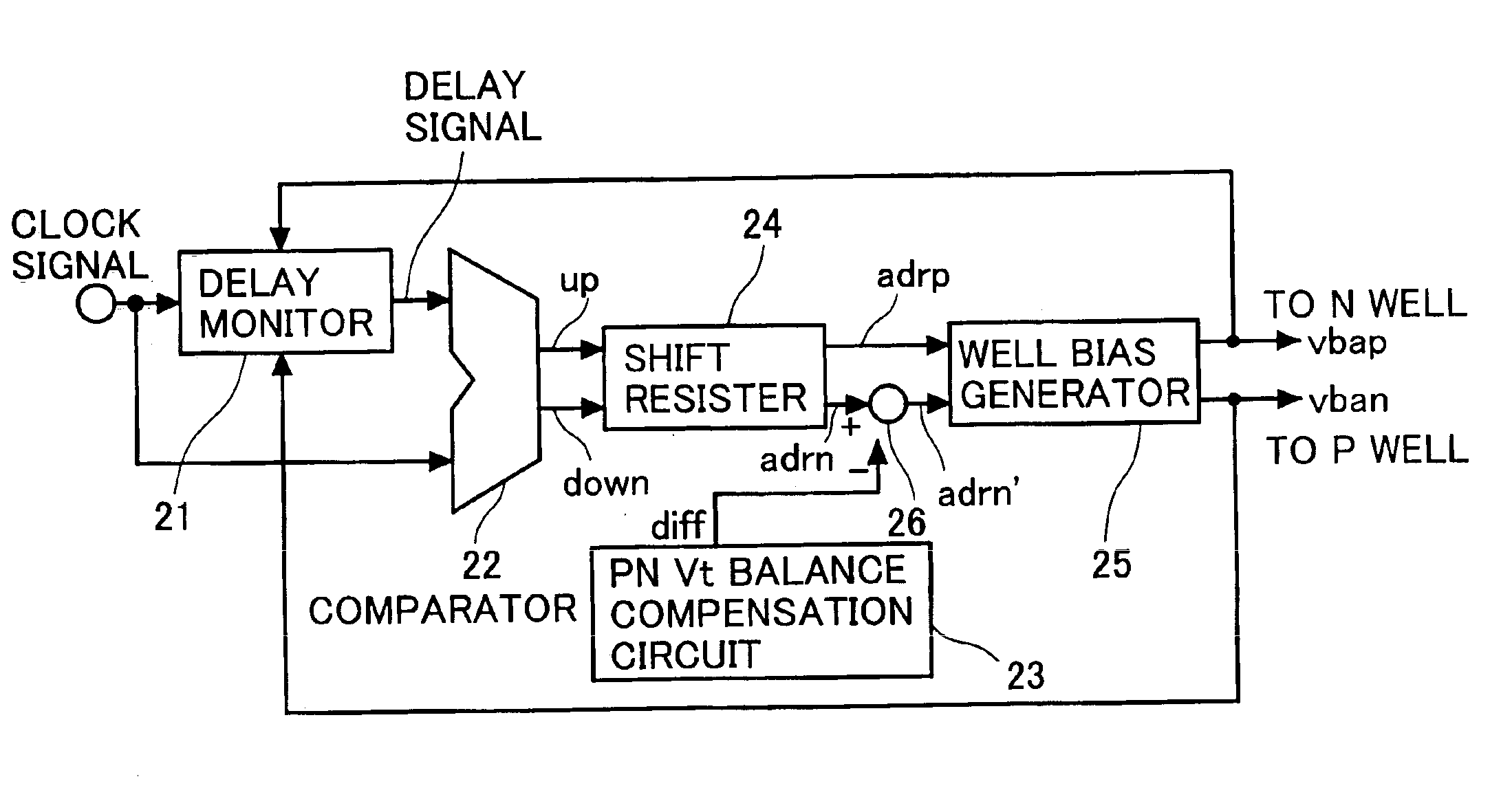
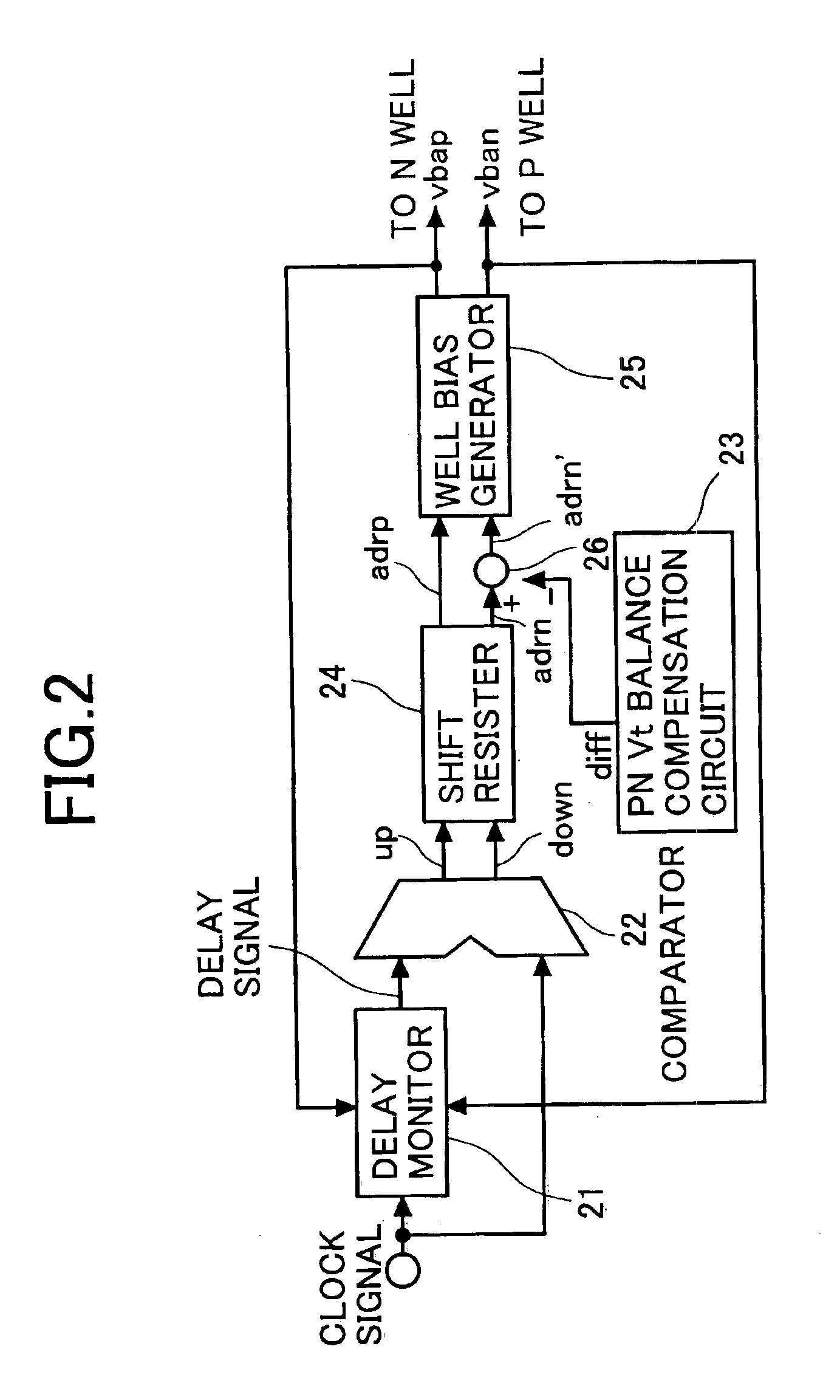
FIG. 2 is a block diagram showing a first embodiment of the control circuit 11 illustrated in FIG. 1. In the embodiment, the control circuit 11 is constructed by a delay monitor 21, a comparator 22, a PN Vt balance compensation circuit 23, a shift register 24, a well bias generator 25, and an adder 26.

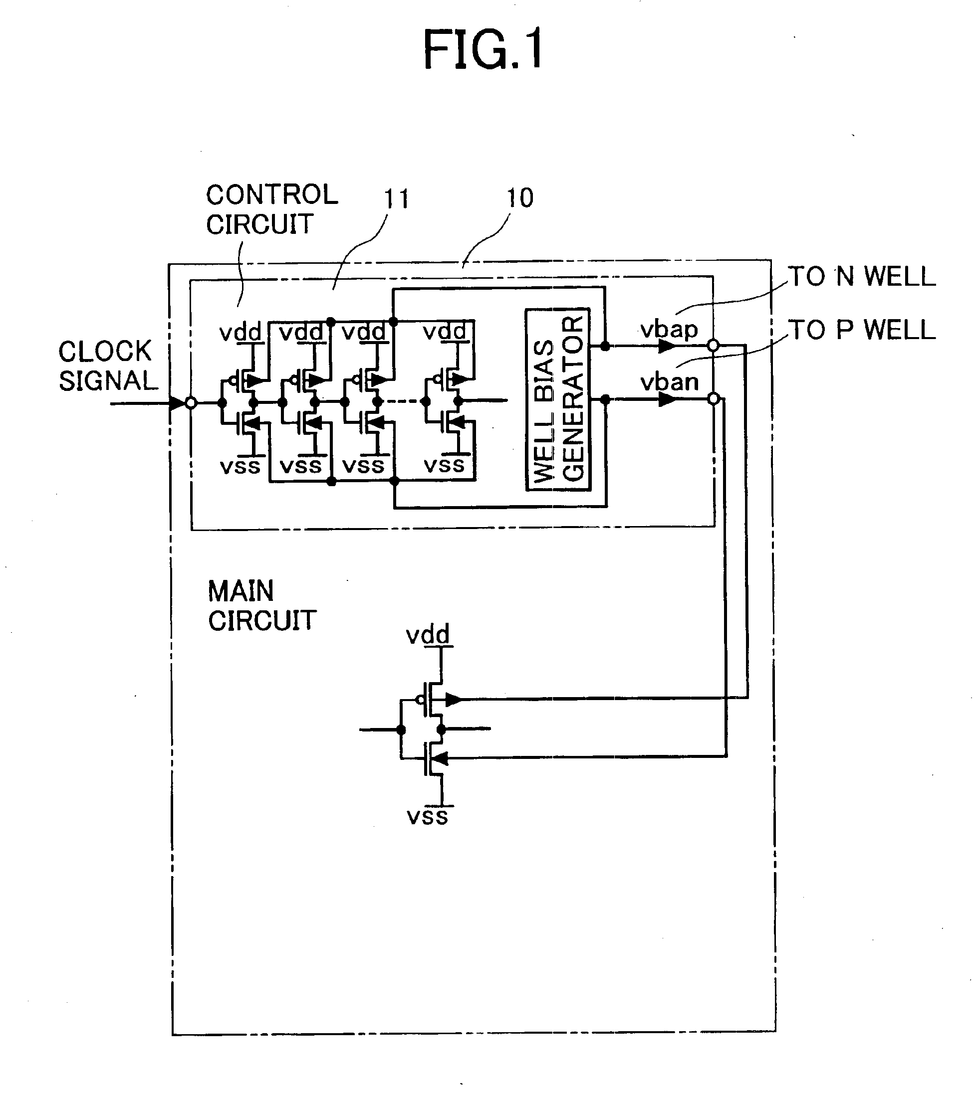
The delay monitor 21 is, as described above, to simulate a critical path of the main circuit 10 and receives a clock signal. The clock signal is a clock signal of the main circuit 10. From the delay monitor 21, therefore, a clock signal having a delay corresponding to delay time of the critical path of the main circuit 10 is obtained as a delay signal. The delay signal of the delay monitor 21 and the clock signal are supplied to the comparator 22. The comparator 22 compares the signals to detect a phase difference and outputs a signal “up” when the delay time is shorter than a design parameter or a signal “down” when the delay time is longer than the design parameter. The shift registe...

embodiment ii

FIG. 12 is a block diagram showing a second embodiment of the control circuit 11 illustrated in FIG. 1. In the embodiment, the control circuit 11 is constructed by the delay monitor 21, comparator 22, PN Vt balance compensation circuit 123, shift register 24, well bias generator 25, and adder 26.

As easily understood from comparison between FIGS. 12 and 2, the control circuit 11 of second embodiment has the same configuration as that of the first embodiment except for the point that the N well voltage vbap is applied to the PN Vt balance compensation circuit 123. The basic operation is the same as that of the first embodiment. FIG. 13 is a block diagram showing an example of the PN Vt balance compensation circuit 123 in FIG. 12. The PN Vt balance compensation circuit 123 is constructed by a logical threshold voltage detector 131, the reference voltage generator 32, comparator 33, difference detector 34, and well bias generator 35 for PN Vt balance. As easily understood from compariso...

embodiment iii

FIG. 15 is a block diagram showing a third embodiment of the control circuit 11 illustrated in FIG. 1. In the embodiment, the control circuit 11 is constructed by the delay monitor 21, comparator 22, PN Vt balance compensation circuit 23, shift register 24, and a well bias generator 1525.

As easily understood from comparison between FIG. 15 and FIGS. 2 and 12, the control circuit 11 of the third embodiment has the same configuration as that of the first or second embodiment except for the point that outputs of the shift register 24 and the PN Vt balance compensation circuit 23 are directly applied to the well bias generator 1525. The basic operation is the same as that of the first or second embodiment. In the third embodiment, in place of modifying the output of the well bias generator 25 according to the output of the shift register 24 by the adder 26 with an output of the PN Vt balance compensation circuit 23, an output of the well bias generator 1525 is obtained by a table lookup...


PUM


Abstract

A semiconductor integrated circuit device having a mechanism of compensating not only circuit operational speed but also variations in leakage current, which includes: a main circuit constructed with CMOS device, a delay monitor for simulating a critical path of the main circuit constructed by a CMOS and monitoring a delay of the path, a PN Vt balance compensation circuit for detecting a threshold voltage difference between a PMOS transistor and an NMOS transistor, and a well bias generating circuit for receiving outputs of the delay monitor and the PN Vt balance compensation circuit and applying a well bias to the delay monitor and the main circuit so as to compensate the operation speed of the delay monitor to a desired speed and reduce a threshold voltage difference between the PMOS and NMOS transistors.

Description

BACKGROUND OF THE INVENTIONIn the second embodiment, in a manner similar to the first embodiment, the delay of the CMOS LSI can be compensated and the threshold voltage difference between the PMOS transistor and the NMOS transistor can be eliminated. In addition, by feeding back the signal vbap to the PN Vt balance compensation circuit 123, even if the threshold voltage difference occurs between the PMOS transistor and the NMOS transistor at the time of changing the signals vbap and vban in order to compensate delay, the difference can be compensated.SUMMARY OF THE INVENTIONWhen the performance of a transistor varies according to a fabricating process and a difference occurs between a threshold voltage of a PMOS transistor and a threshold voltage of an NMOS transistor, even if the circuit speed is the same, leakage currents of the circuits may differ from each other. This happens for the reason that the leakage current depends on, not the circuit operation speed, but a threshold vol...

Claims


Application Information

Patent Timeline
Patent Type & Authority Patents(United States)
IPC IPC(8): H03K19/003H01L21/822G11C11/40H01L21/8238H01L27/04H01L27/092H03K17/30
CPCH03K19/00384H03K2217/0018G11C11/40
Inventor ONO, GOICHIMIYAZAKI, MASAYUKIISHIBASHI, KOICHIRO
Owner RENESAS ELECTRONICS CORP
Why Eureka
Try Eureka