

Semiconductor memory device and control method thereof
a memory device and semiconductor technology, applied in the direction of digital storage, electrical equipment, instruments, etc., can solve the problems of data disappearance, data cannot be read out of memory cells c, data is garbled, etc., and achieve the effect of short time, sufficient time for cessation, and short tim
- Summary
- Abstract
- Description
- Claims
- Application Information
AI Technical Summary
Benefits of technology
Problems solved by technology
Method used
Image

Examples
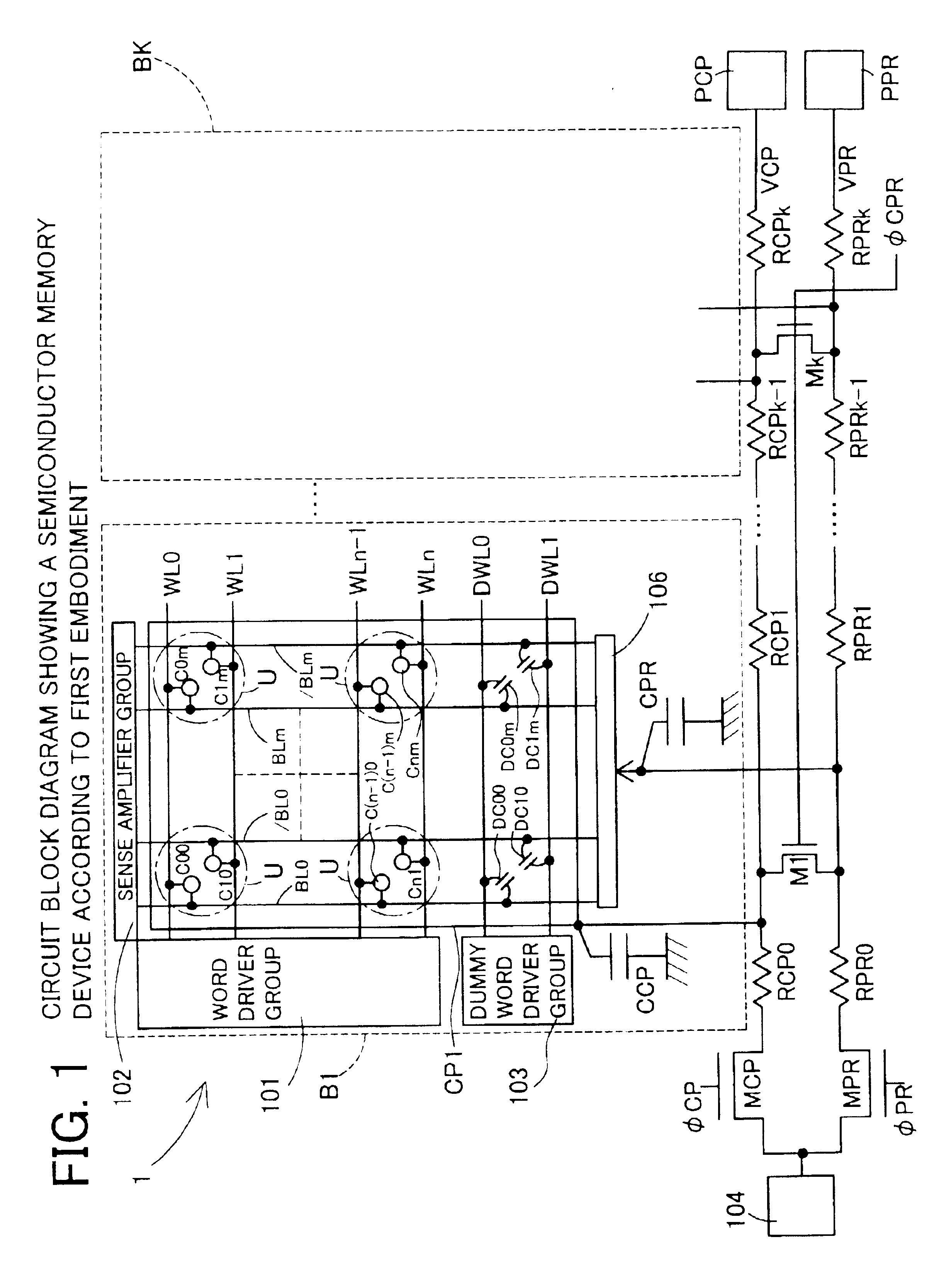
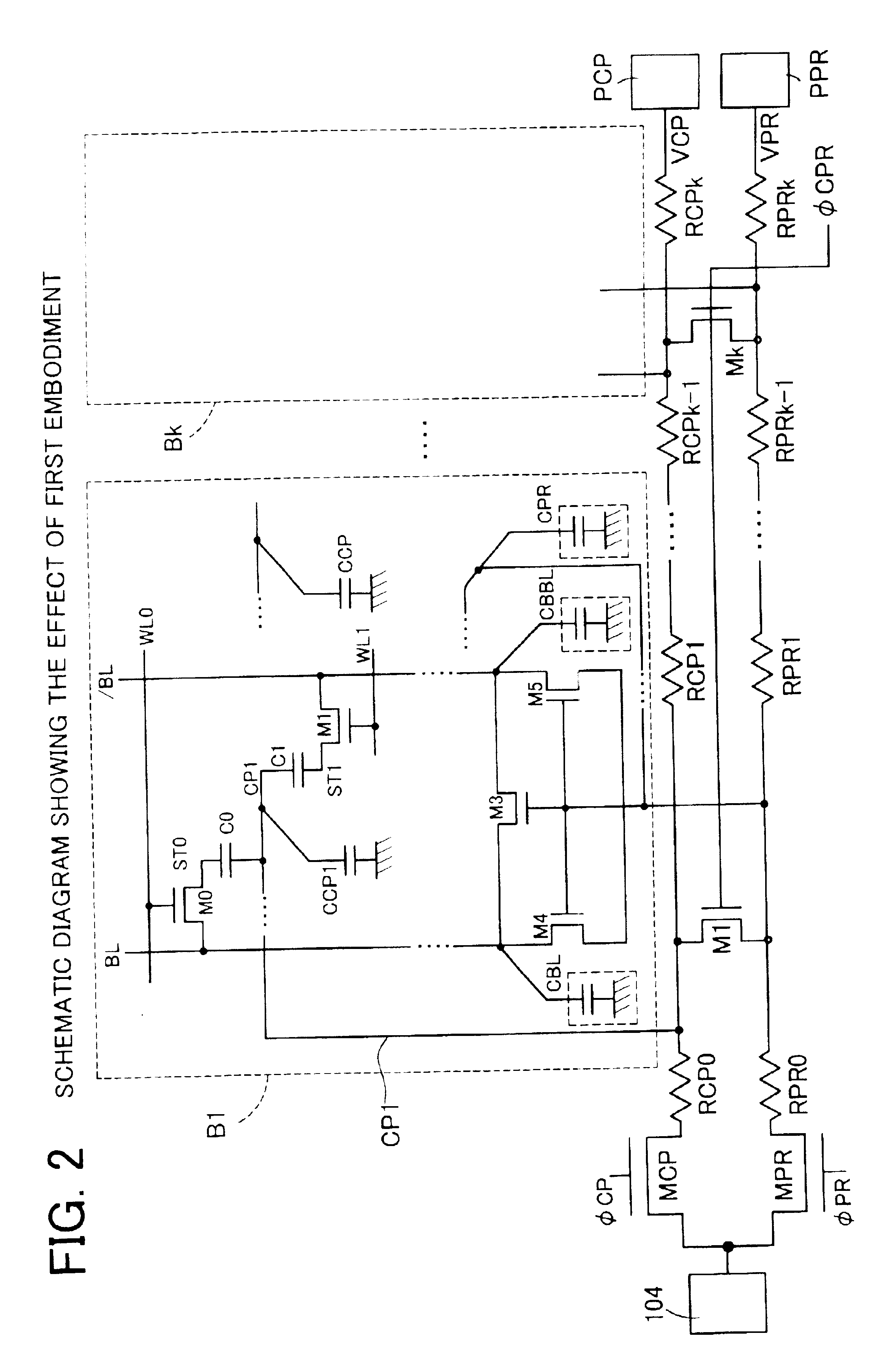
first embodiment
A semiconductor memory device 1 (hereinafter referred to as a DRAM 1) according to the invention shown in FIG. 1 comprises NMOS transistors M1 to Mk for connecting both a line VPR and a line VCP as feeders for reference voltages VPR, VCP from a reference voltage generation circuit 104 in each cell block B1 to Bk, in addition to the configuration of the DRAM 1000 according to a conventional art (see FIG. 15).
Gate terminals of the NMOS transistors M1 to Mk are connected to a common signal φCPR. The signal φCPR outputs a positive logical level at a predetermined time after power-on. A circuit for generating the signal φCPR can use an output signal from a power-on reset circuit for detecting power-on and outputting a pulse signal for a predetermined time period. In addition, a circuit which has a response characteristic of delaying only a trailing edge of the pulse signal can be added as a circuit for receiving the output signal from the power-on reset circuit and extending the pulse wi...
second embodiment
In a semiconductor memory device 2 (hereinafter referred to as a DRAM 2) according to the invention shown in FIG. 3, a reference voltage generation portion 104B and reference voltage drive portions 104D to 104D which are constituents of the reference voltage generation circuit 104 of the DRAM 1000 according to the conventional art (see FIG. 15) are divided and arranged, instead of the reference voltage generation circuit 104. The reference voltage drive portions 104D to 104D are dispersedly distributed to each cell block B1 to Bk to supply a voltage VCP to each cell plate CP1 to CP1 in each cell block B1 to Bk. The reference voltage generation portion 104B outputs a reference voltage value signal for setting the reference voltage to be supplied by the reference voltage drive portions 104D to 104D. Signals output from a connection point between MOS transistors M6 and M7 and a connection point between MOS transistors M8 and M9 are input as bias signals to each gate terminal of NMOS tr...
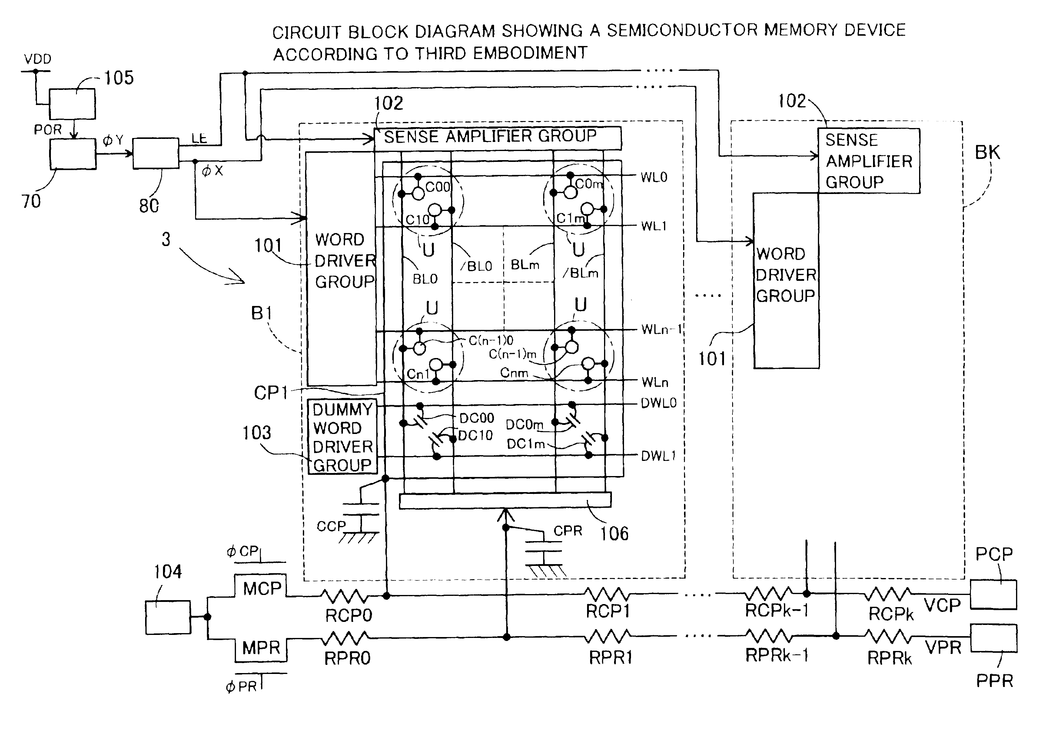
third embodiment
A semiconductor memory device 3 (hereinafter referred to as a DRAM 3) according to the invention shown in FIG. 4 comprises a power supply detection circuit 105 for detecting the input of a power supply voltage, a pulse extension circuit 70 for extending the pulse width of a pulse output signal POR from the power supply detection circuit 105, and a control circuit 80 for operating in response to an output signal φY from the pulse extension circuit 70, in addition to the configuration of the DRAM 1000 according to the conventional art (see FIG. 15). The control circuit 80 outputs a sense amplifier group activation signal LE together with a word line activation signal φX. Both signals are output to each cell block B1 to Bk. As the power supply detection circuit 105 and the pulse width expansion circuit 70, existing circuits can be used. For example, the power supply detection circuit 105 is a power-on reset circuit, and outputs a positive pulse signal POR as its output signal at power-...
PUM
 Abstract
Description
Claims
Application Information