

Method of fabricating a multilayer dielectric tunnel barrier structure
a tunnel barrier and dielectric tunnel technology, applied in the field of semiconductor/solid-state device details, semiconductor memory, sensor applications, etc., can solve the problems of reducing the ratio of magnetoresistance between interfaces and substrates, difficult to consistently produce devices with nearly the same resistance over typical substrate sizes currently used, and oxidation process creating anomalous effects, etc., to achieve good deposition conformality, reduce resistance, reduce or eliminate pinhole formation and breakdown areas
- Summary
- Abstract
- Description
- Claims
- Application Information
AI Technical Summary
Benefits of technology
Problems solved by technology
Method used
Image

Examples
Embodiment Construction
The present invention will be understood from the following detailed discussion of the exemplary embodiments which is presented in connection with the accompanying drawings.
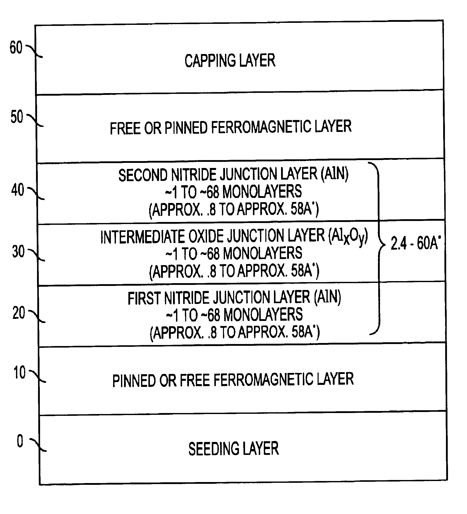
The present invention provides a multilayer dielectric tunnel barrier used in magnetic tunnel junction devices and its method of fabrication. The multilayer film has lower barrier layer resistance, is very conformal, and can be made as a thicker or thinner film with fewer pinholes.
In the following description, specific details such as layer thicknesses, process sequences, and material compositions are set forth to provide a complete understanding of the present invention. However, it will be obvious to one skilled in the art that the present invention can be employed without using such specific details. In addition, in order for a simplified description, techniques, processes, and equipment that are well-known in the art have not been described in detail.
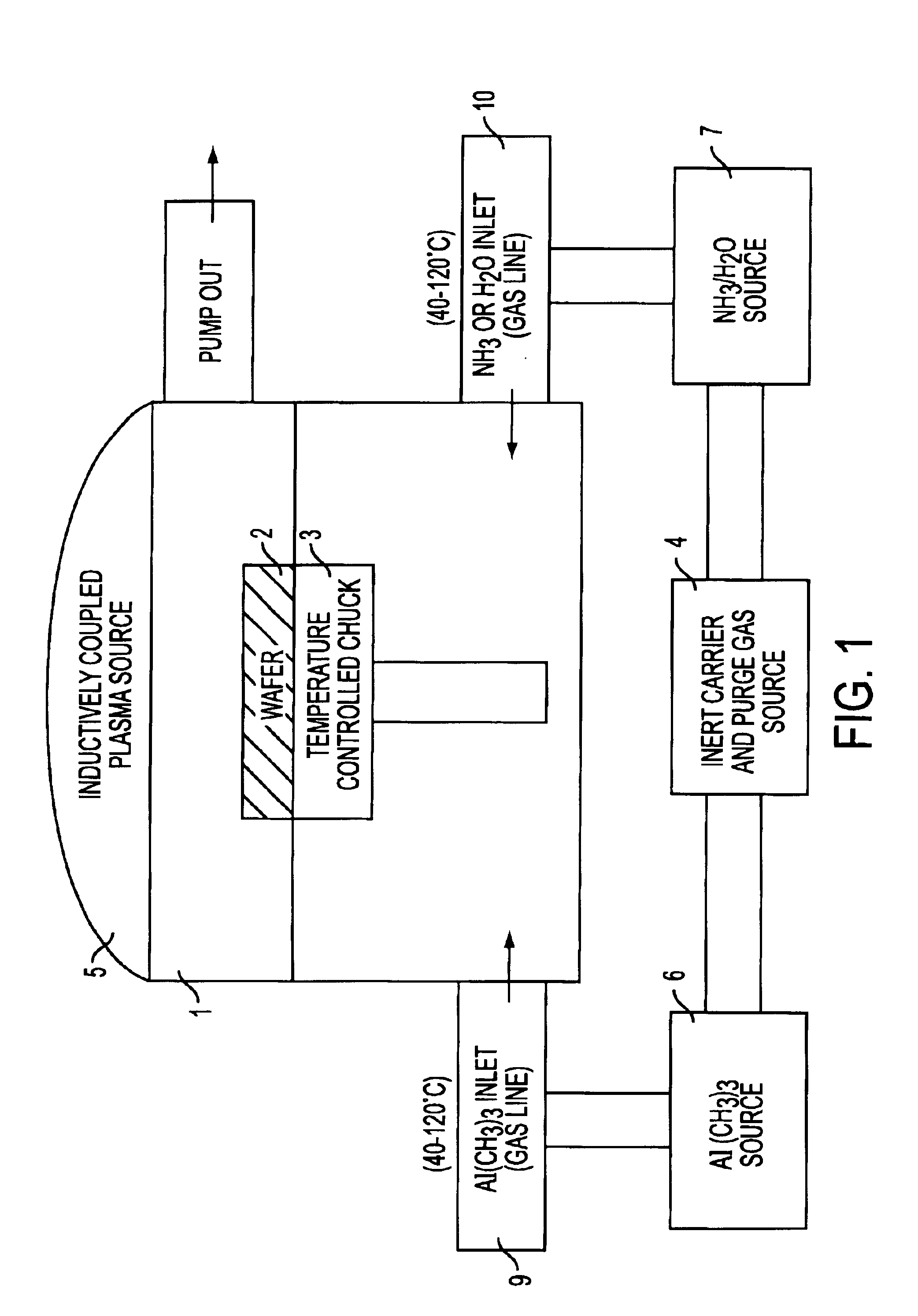
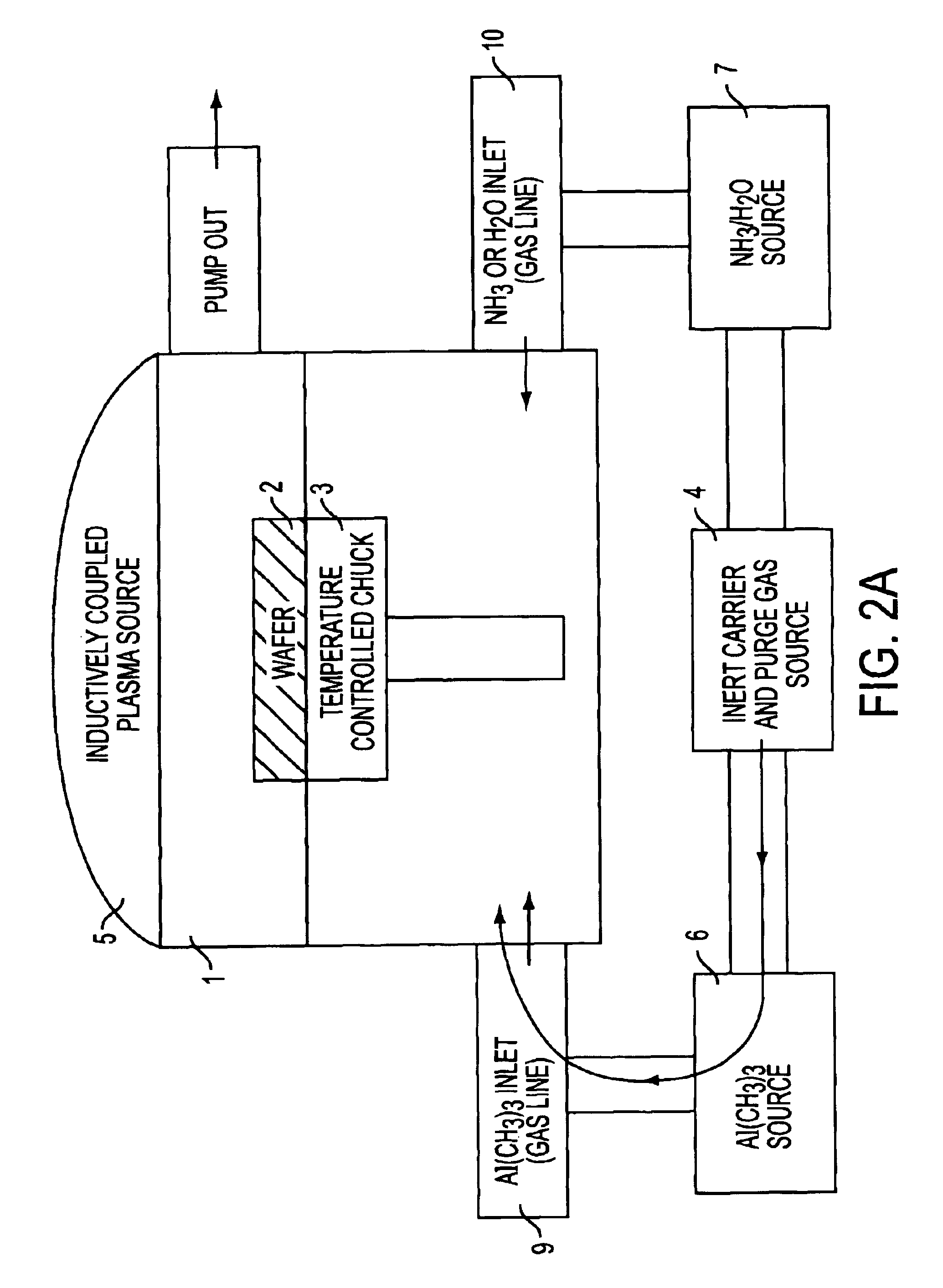
For purposes of the present invention, the tunnel barrier i...
PUM
| Property | Measurement | Unit |
|---|---|---|
| temperature | aaaaa | aaaaa |
| temperature | aaaaa | aaaaa |
| temperature | aaaaa | aaaaa |
Abstract
Description
Claims
Application Information