Method for fabricating flash memory

Inactive Publication Date: 2005-02-01
MACRONIX INT CO LTD
View PDF5 Cites 9 Cited by
  • Summary
  • Abstract
  • Description
  • Claims
  • Application Information

AI Technical Summary

Benefits of technology

To solve the above-mentioned problems of the prior art, this invention provides a method for fabricat

Problems solved by technology

The disadvantage of the conventional flash memory is that a leakage easily occurs in the memory cell if there are weak points in the tunnel oxide layer, and the reliability of the device is thus lowered.
A leakage therefore does not

Method used


Image

  • Method for fabricating flash memory
  • Method for fabricating flash memory
  • Method for fabricating flash memory

Examples


Embodiment Construction

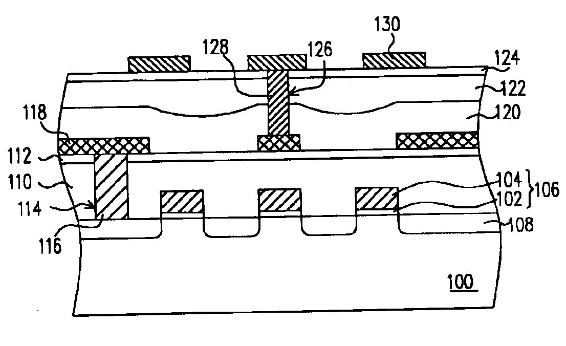
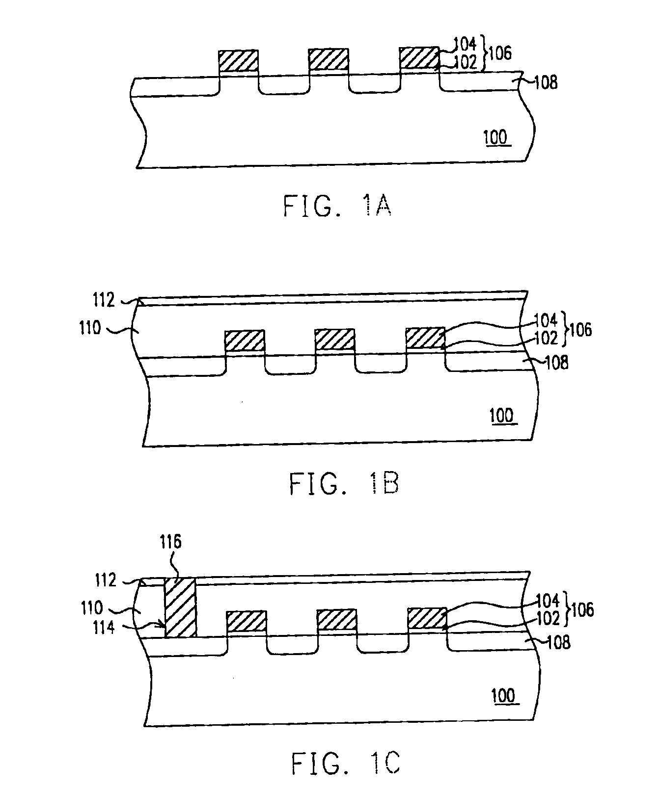
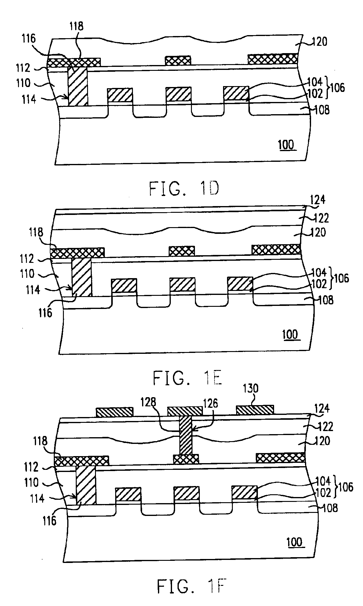
Referring now to FIGS. 1A˜1F, the process flow of fabricating a flash memory according to a preferred embodiment of this invention will be described hereafter.

Refer to FIG. 1A, a substrate 100, such as a silicon substrate, is provided and then a composite dielectric layer 102 and a gate conductive layer 104 are sequentially formed on the substrate 100. The composite dielectric layer 102 may have a silicon oxide / silicon nitride / silicon oxide (ONO) structure comprising a tunnel oxide layer, a nitride charge-trapping layer, and a silicon oxide layer. The gate conductive layer 104 is, for example, a polycide layer comprising a doped polysilicon layer and a metal silicide layer such as a tungsten silicide layer. The doped polysilicon layer is formed by, for example, chemical vapor deposition (CVD) with in-situ doping. The tungsten silicide is formed by, for example, low pressure chemical vapor deposition (LPCVD) with WF6 and SiH4 as reaction gases.

The gate conductive layer 104 and the co...


PUM


Abstract

A method for fabricating a flash memory is described. A stacked gate structure and a source/drain are formed on a substrate. An inter-layer dielectrics and a plurality of inter-metal dielectric layers are then formed over the substrate, wherein at least one layer among the inter-layer dielectrics and the inter-metal dielectric layers has a silicon carbide layer formed thereon. The silicon carbide layer is formed to protect the memory device from an UV irradiation, so as to prevent data errors occurring in the memory device.

Description

BACKGROUND OF INVENTION1. Field of InventionThe present invention relates to a method for fabricating a non-volatile memory (NVM). Particularly, the present invention relates to a method for fabricating a flash memory.2. Description of Related ArtFlash memory is a type of electrically erasable programmable read-only memory (E2 PROM). A flash memory can be programmed, read, and erased repeatedly and can retain data even if power is switched off, and therefore is widely used in personal computers and in electronic apparatuses.A conventional flash memory uses a floating gate and a control gate both made from doped polysilicon. When the flash memory is to be programmed, the control gate and the source / drain of a selected memory cell are applied with appropriate biases. An electron flow from the source to the drain is thereby induced in the channel. The electron flow can produce hot electrons that will tunnel through the tunnel oxide layer and into the floating gate and will distribute e...

Claims


Application Information

Patent Timeline
IPC IPC(8): H01L27/115H01L21/70H01L21/8247
CPCH01L27/115H01L27/11521Y10S438/931H10B69/00H10B41/30
Inventor CHANG, PING-YIJENG, PEI-REN
Owner MACRONIX INT CO LTD
Why Eureka
Try Eureka