Method and device for forming an STI type isolation in a semiconductor device

a semiconductor device and trench isolation technology, applied in semiconductor/solid-state device manufacturing, basic electric elements, electric devices, etc., can solve the problems of isolation regions, narrow silicon substrates, and reduced device operation efficiency, and achieve enhanced device characteristics and leakage current during device operation.

Inactive Publication Date: 2005-02-01
SAMSUNG ELECTRONICS CO LTD
View PDF15 Cites 39 Cited by
  • Summary
  • Abstract
  • Description
  • Claims
  • Application Information

AI Technical Summary

Benefits of technology

It is therefore a feature of an embodiment of the present invention to provide an STI type semiconductor device and a method for manufacturing an STI type semiconductor device with enhanced device characteristics, whereby a leakage current during device operation and a charge leak from a capacitor may be reduced.

Problems solved by technology

Also, isolation regions, which play an important role in preventing current leakage between two adjacent devices, become narrow.
High integration of the devices may cause several problems.
Usually, the silicon substrate, which was exposed by the anisotropic etching process, has many crystal defects caused by the anisotropic dry etching process.
Therefore, a thermal oxide is formed on the silicon substrate, but many crystal defects may still exist between the thermal oxide layer and the silicon substrate.
Defects in the silicon substrate move easily so that the morphology of the trench sidewall deteriorates and dislocations occur easily.
Additionally, dangling bonds that exist in the crystal defect become trap sites of electrical charges, thereby causing a leakage current during memory cell device operation.

Method used


Image

  • Method and device for forming an STI type isolation in a semiconductor device
  • Method and device for forming an STI type isolation in a semiconductor device
  • Method and device for forming an STI type isolation in a semiconductor device

Examples


embodiment 1

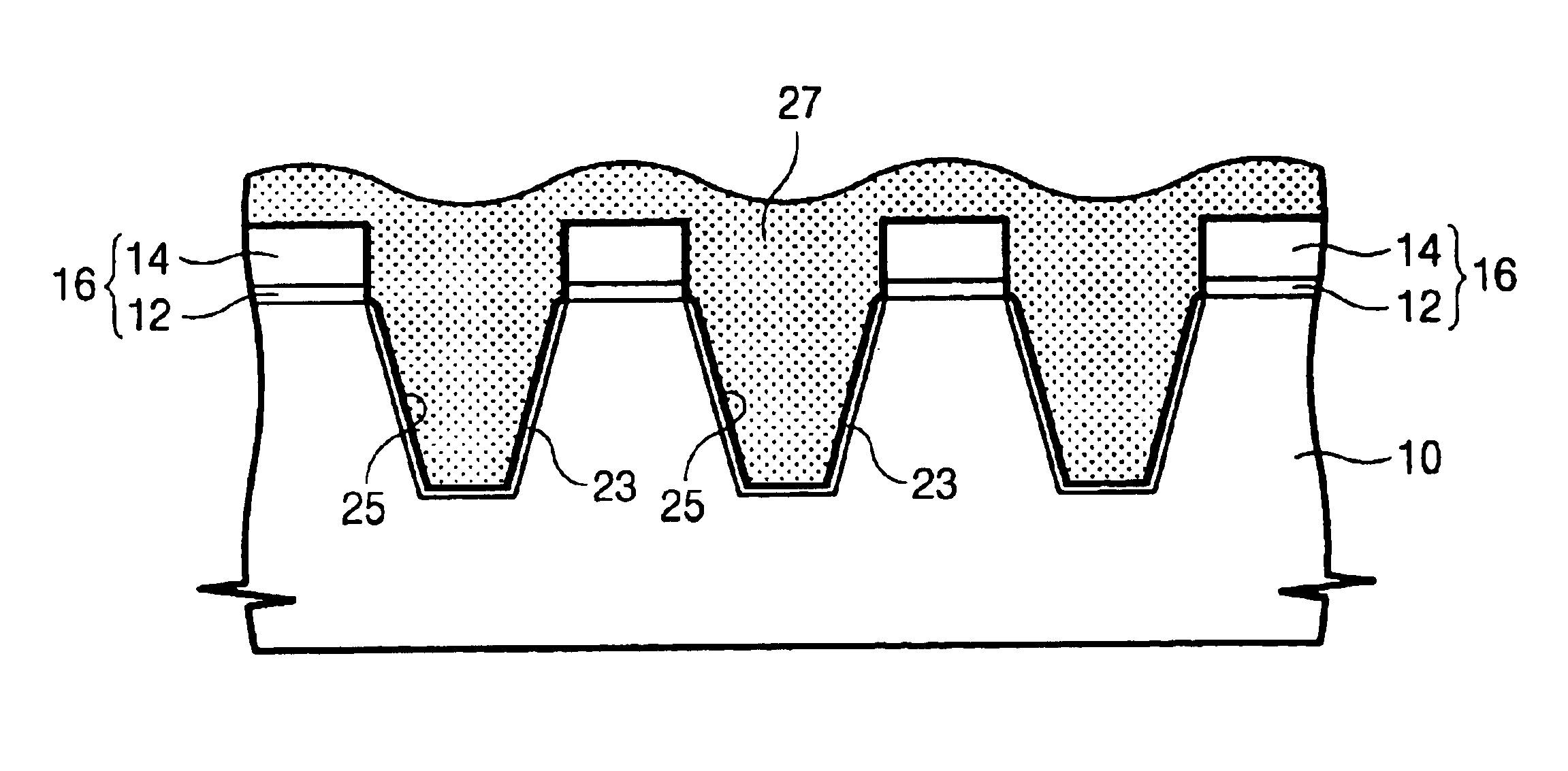
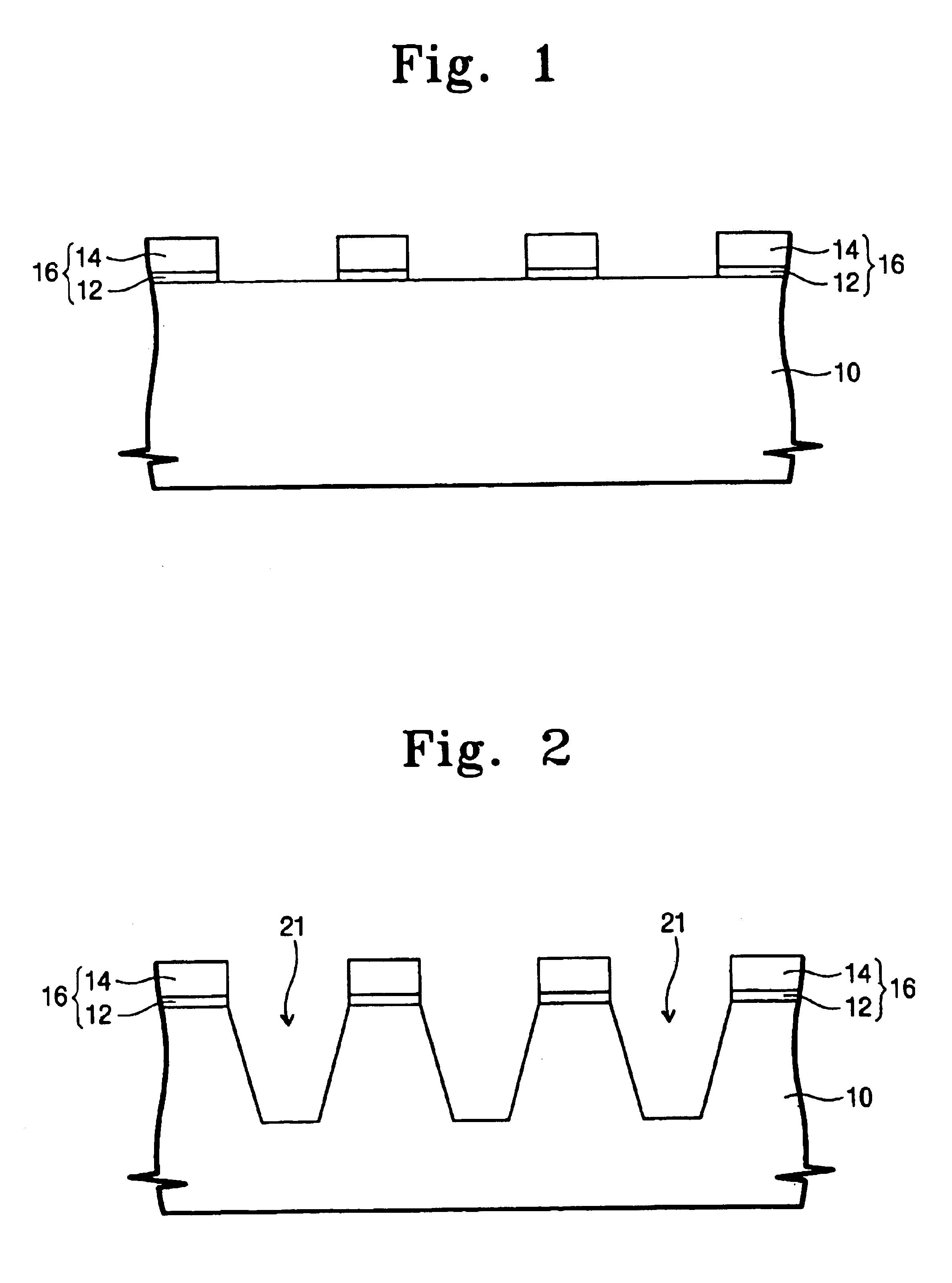
FIG. 1-FIG. 5 show cross-sectional views of a semiconductor device setting forth stages in a manufacturing process for forming a trench isolation in accordance with an embodiment of the present invention. FIG. 1 shows a trench etching mask (16) which is made of a pad oxide layer (12) and silicon nitride layer (14) on a silicon substrate (10). Specifically, the pad oxide layer (12) is formed on the silicon substrate (10) and the silicon nitride layer (14), which acts as an etching prevention or barrier layer, is deposited by CVD. A photoresist pattern for a trench is formed by a photolithography process. The silicon nitride layer (14) and pad oxide layer (12) are etched through and the photoresist pattern is removed, thereby forming the trench etching mask (16).

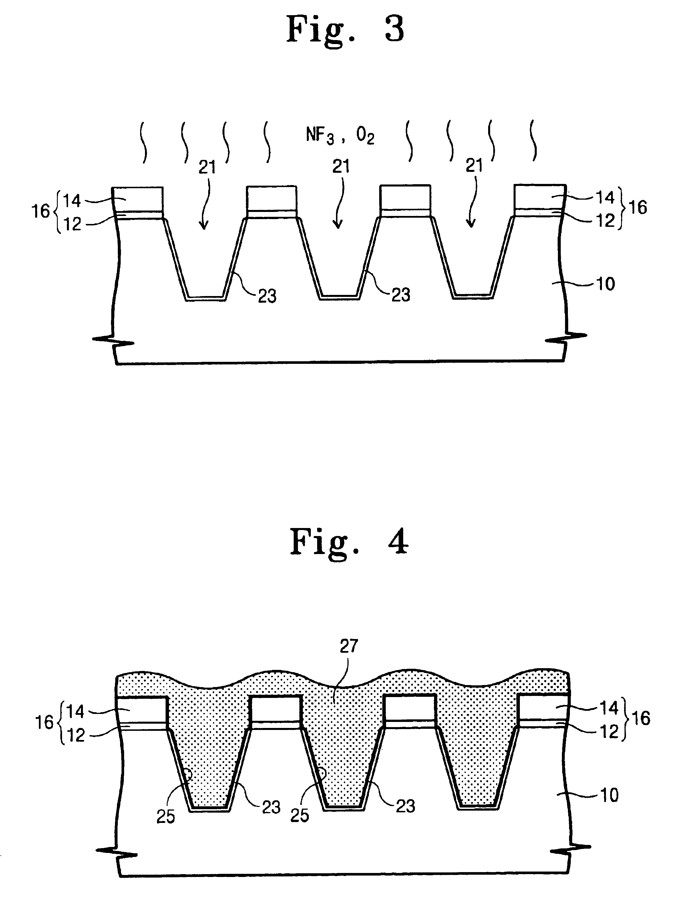
FIG. 2 shows an etching of a silicon substrate (10) using the trench etching mask (16) thereby forming a trench (21) in the silicon substrate. Preferably, etching the silicon substrate is accomplished by an anisotropic etch, a...

embodiment 2

The process of embodiment 2 is similar to that of embodiment 1, with the exception of the method of supplying fluorine gas. Unlike embodiment 1, fluorine gas is not supplied to the interface between the trench device isolation layer (29) and the substrate (10) during thermal oxidation of the trench sidewall. In embodiment 2, the simultaneous processes shown in FIG. 3 of embodiment 1, including both thermal oxidation and supplication of fluorine gas or NF3 containing fluorine, are divided into two steps, as shown in FIG. 6 and FIG. 7.

Referring to FIG. 6, the substrate (10) where the trench (21) is formed is thermally oxidized in a furnace to form silicon thermal oxide without fluorine. In other words, a sidewall thermal oxide layer (23′) is formed inside the trench (21).

Referring to FIG. 6 and FIG. 7, the sidewall thermal oxide layer (23′) on the sidewall inside the trench is annealed in a process which additionally supplies a fluorine containing gas, such as NF3 gas. Fluorine, disso...


PUM


Abstract

A trench isolation in a semiconductor device, and a method for fabricating the same, includes: forming a trench having inner sidewalls for device isolation in a silicon substrate; forming an oxide layer on a surface of the silicon substrate that forms the inner sidewalls of the trench; supplying healing elements to the silicon substrate to remove dangling bonds; and filling the trench with a device isolation layer, thereby forming the trench isolation without dangling bonds causing electrical charge traps.

Description

BACKGROUND OF THE INVENTION1. Field of the InventionThe present invention relates to a Shallow Trench Isolation (STI) type semiconductor device and a method for manufacturing an STI type semiconductor device. More particularly, the present invention relates to a method for manufacturing an STI type semiconductor device wherein the interface between a silicon substrate and a device isolation layer has enhanced electrical characteristics so that a leakage current may be reduced.2. Description of the Related ArtAs is well known in the art, a dynamic random access memory (DRAM) having a memory cell comprising a transistor and a capacitor may be downsized to produce a higher degree of integration in the DRAM.Accordingly, as device dimensions of the memory cell are reduced, the dimensions of active regions and the space therebetween are reduced as well. Also, isolation regions, which play an important role in preventing current leakage between two adjacent devices, become narrow. High int...

Claims


Application Information

Patent Timeline
Patent Type & Authority Patents(United States)
IPC IPC(8): H01L21/762H01L21/70H01L21/76
CPCH01L21/76224H01L21/76
Inventor KIM, CHUL-SUNGCHOI, SI-YOUNGPARK, JUNG-WOORYU, JONG-RYOLLEE, BYEONG-CHAN
Owner SAMSUNG ELECTRONICS CO LTD
Why Eureka
Try Eureka