Phosphoric acid free process for polysilicon gate definition

a technology of polysilicon gate and phosphoric acid, which is applied in the direction of semiconductor devices, basic electric elements, electrical equipment, etc., can solve problems such as yield loss, and achieve the effect of preventing particle contamination and improving the control of critical dimensions

Inactive Publication Date: 2005-02-01
TAIWAN SEMICON MFG CO LTD
View PDF11 Cites 16 Cited by
  • Summary
  • Abstract
  • Description
  • Claims
  • Application Information

AI Technical Summary

Benefits of technology

[0008]It is another object of this invention to employ a photolithographic procedure featuring a dual anti-reflective coating (ARC), to improve the control of the critical dimension, a narrow width polysilicon gate structure, obtained via dry etching procedures.
[0009]It is still another object of this invention to remove dual ARC layers comprised of an underlying dielectric ARC (DARC) layer and an overlying organic bottom ARC (BARC) layer, without the use of hot phosphoric acid, preventing particle contamination of the in-process MOSFET device sometimes encountered in hot phosphoric acid baths.

Problems solved by technology

However the hot phosphoric wet etch tanks if not frequently maintained can be loaded with unwanted particles as a result of previous applications.
After DARC removal particles from the contaminated hot phosphoric acid wet etch tank can deposit on critical regions of the in-process MOSFET device resulting in yield loss.

Method used


Image

  • Phosphoric acid free process for polysilicon gate definition
  • Phosphoric acid free process for polysilicon gate definition
  • Phosphoric acid free process for polysilicon gate definition

Examples


Embodiment Construction

ectional style, describe key stages used to define a MOSFET polysilicon gate structure wherein a dual ARC coating, used to enhance dimension control of the polysilicon gate structure, is removed without the use of hot phosphoric acid.

DESCRIPTION OF THE PREFERRED EMBODIMENTS

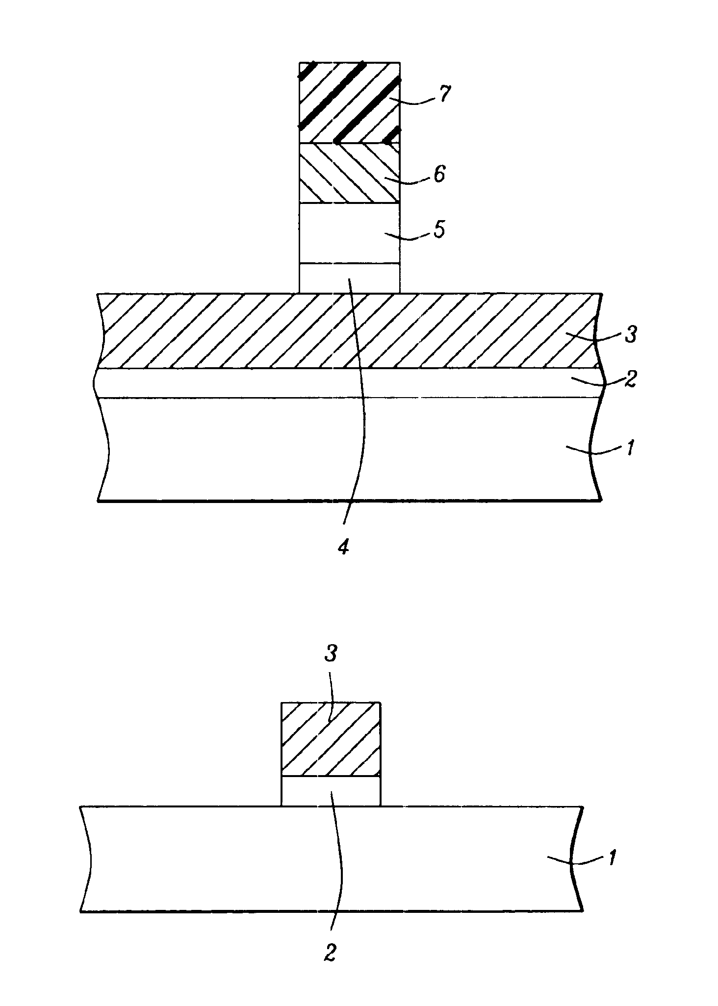
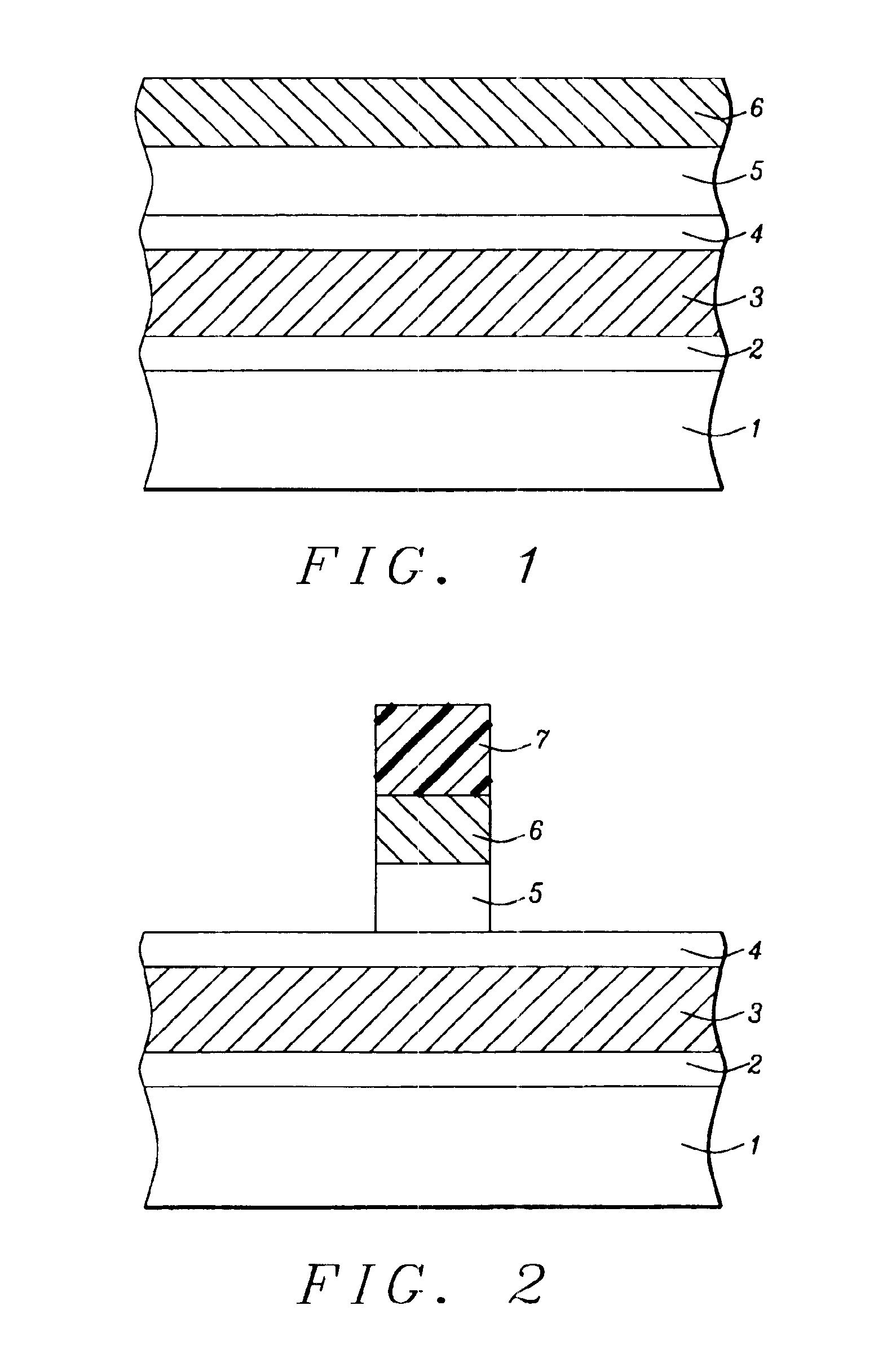
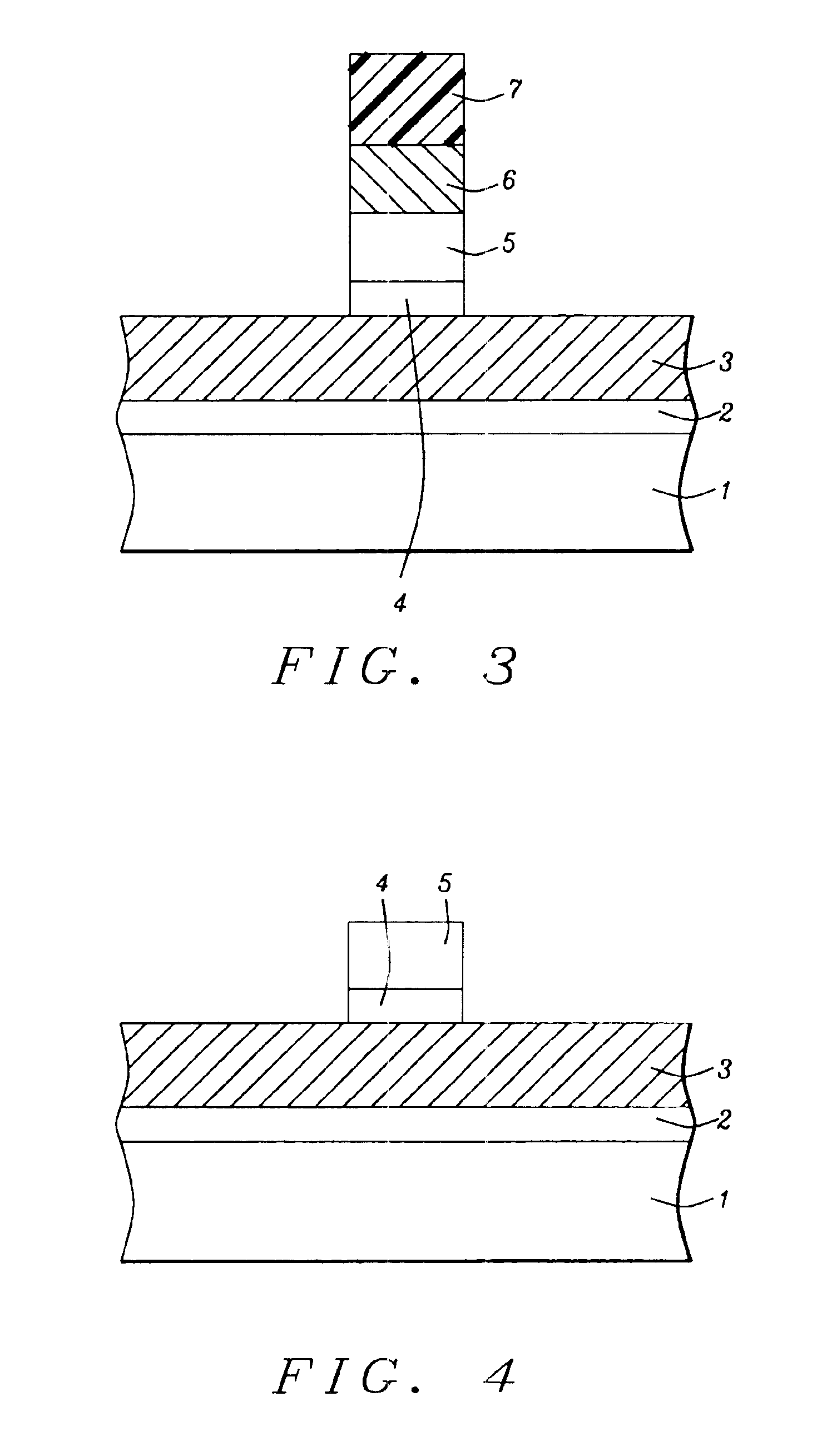
[0013]The method of defining a polysilicon gate structure for a MOSFET device wherein a dual ARC coating is employed as a component of the defining photolithographic procedure, and wherein the dual ARC coating is removed without the use of hot phosphoric acid, will now be described in detail. Semiconductor substrate 1, comprised if P type single crystalline silicon featuring a crystallographic orientation, is used and schematically shown in FIG. 1. Gate insulator 2, comprised of a gate dielectric layer such as thermally grown silicon oxide, silicon oxynitride, nitrogen doped silicon oxide or a high dielectric constant (high k) layer, is formed to a thickness between about 6 to 80 Angstroms on semiconductor substr...


PUM


Abstract

A method of defining a gate structure for a MOSFET device featuring the employment of dual anti-reflective coating (ARC) layers to enhance gate structure resolution, and featuring a dry procedure for removal of all ARC layers avoiding the use of hot phosphoric acid, has been developed. After formation of a polysilicon layer on an underlying silicon dioxide gate insulator layer, a capping silicon oxide, a dielectric ARC layer, and an overlying organic ARC layer are deposited. A photoresist shape is formed and used as an etch mask to allow a first anisotropic RIE procedure to define the desired gate structure shape in the dual ARC layers and in the capping silicon oxide layer. After removal of the photoresist shape and the overlying organic ARC layer a second anisotropic RIE procedure is used to define a desired polysilicon gate structure, with the second anisotropic RIE procedure also resulting in the removal of the dielectric ARC shape. A final hydrofluoric acid type solution is then used to remove the capping silicon oxide shape as well as to remove the portions of the silicon dioxide gate insulator layer not covered by the polysilicon gate structure.

Description

BACKGROUND OF THE INVENTION[0002](1) Field of the Invention[0003]The present invention relates to methods used to fabricate semiconductor devices, and more specifically to a method used to define a polysilicon gate structure for a metal oxide semiconductor field effect transistor (MOSFET) device.[0004](2) Description of Prior Art[0005]Micro-miniaturization, or the ability to fabricate semiconductor devices with sub-micron features, has allowed the performance of the sub-micron device to be increased while the fabrication cost of the same sub-micron semiconductor device has been decreased. The smaller device features result in decreases in performance degrading parasitic capacitances in addition to allowing a greater number of smaller semiconductor chips, still comprised with device densities comparable to larger semiconductor chips, to be obtained from a specific size starting wafer thus reducing the process cost of each individual semiconductor chip. One critical dimension of sub m...

Claims


Application Information

Patent Timeline
Patent Type & Authority Patents(United States)
IPC IPC(8): H01L21/02H01L21/4763H01L21/302H01L21/336H01L21/70H01L21/8234H01L21/311H01L21/3213H01L29/40
CPCH01L21/31116H01L21/32139H01L21/32137
Inventor LIN, LI-TE S.CHENG, FANG-CHENLIN, HUIN-JERCHIU, YUAN-HUNGTAO, HUN-JAN
Owner TAIWAN SEMICON MFG CO LTD
Why Eureka
Try Eureka