

X-ray flat panel detector
- Summary
- Abstract
- Description
- Claims
- Application Information
AI Technical Summary
Benefits of technology
Problems solved by technology
Method used
Image

Examples
first embodiment
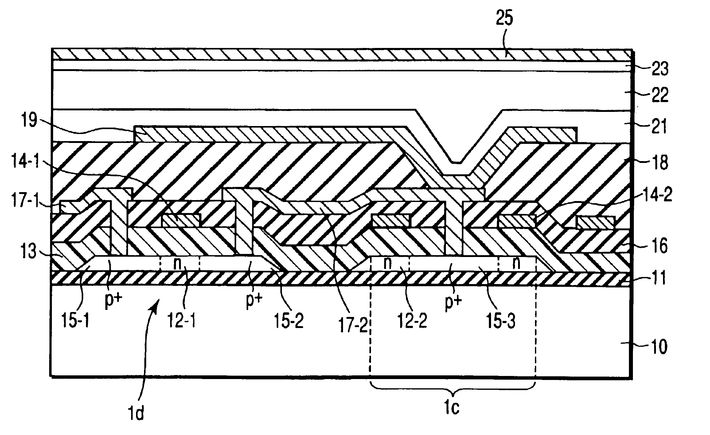
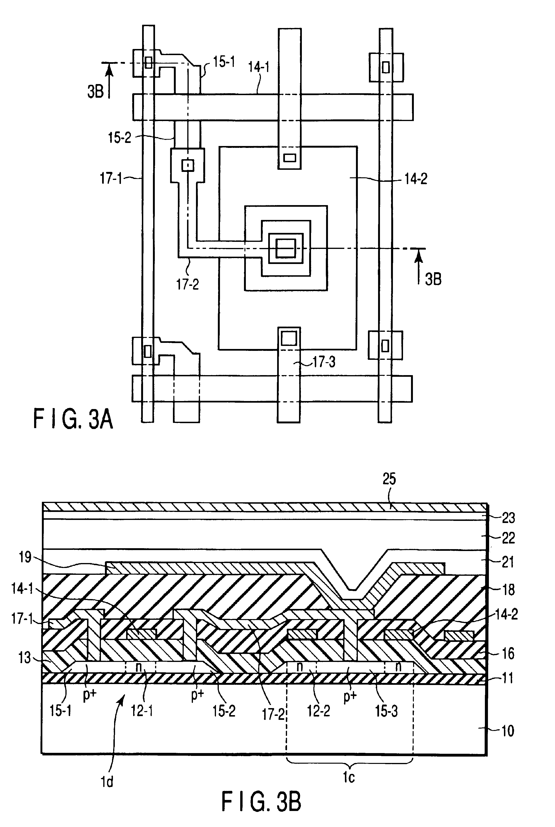
(First Embodiment)
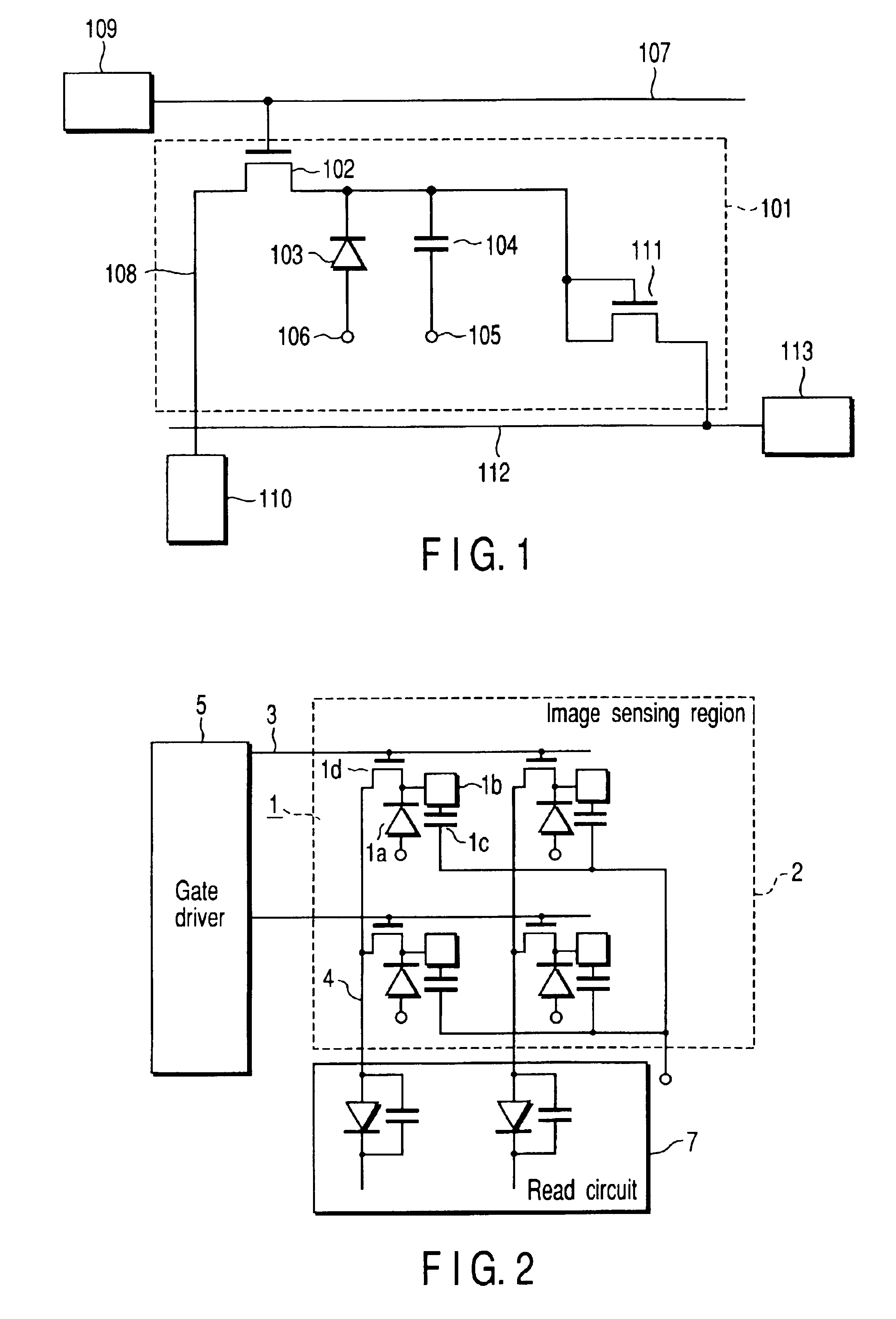
FIG. 2 is a circuit diagram showing the basic arrangement of an X-ray flat panel detector according to the first embodiment of the present invention.
X-ray detection pixels 1 for converting incident X-rays into an electrical signal are two-dimensionally arrayed to form an image sensing region 2. Each pixel 1 comprises an X-ray charge conversion film 1a for converting incident X-rays into an electrical signal, a pixel electrode 1b connected to the X-ray charge conversion film 1a, a storage capacitor 1c connected to the pixel electrode 1b, and a switching thin-film transistor (TFT) 1d having a source connected to the pixel electrode 1b. FIG. 2 shows a simple 2×2 pixel arrangement. In fact, an m×n pixel arrangement including a number of rows and a number of columns is formed.
An important point of the present invention is that the direction of a bias voltage to be applied to the X-ray charge conversion film 1a is selected in accordance with the type of X-ray charge conv...
second embodiment
(Second Embodiment)
FIG. 6A is a plan view showing the structure of one pixel of an X-ray flat panel detector according to the second embodiment of the present invention. FIG. 6B is a sectional view showing the structure of one pixel of the X-ray flat panel detector. The same reference numerals as in FIG. 3A denote the same parts in FIGS. 6A and 6B, and a detailed description thereof will be omitted.
The second embodiment is different from the above-described embodiment in that the switching TFT has an LDD (Lightly Doped Drain) structure. The process until an undercoat insulating film 11, p-Si film 12, gate SiO2 film 13, and gate electrodes 14 are formed on a glass substrate 10 is the same as in the first embodiment.
Next, using the gate electrodes or a resist as a mask, B is doped by ion implantation at 1×1011 cm−2 to 5×1014 cm−2, preferably, 3×1012 cm−2 to 5×1013 cm−2, and in this embodiment, 2×1013 cm−2 to form p−-regions 35-1 and 35-2 of LDDs. This almost corresponds to an impurity...
third embodiment
(Third Embodiment)
FIG. 7 is a circuit diagram showing a driver circuit in an X-ray flat panel detector according to the third embodiment of the present invention. FIG. 8 is a sectional view of the driver circuit. The same reference numerals as in FIG. 3B denote the same parts in FIG. 8, and a detailed description thereof will be omitted.
In this embodiment, a driver circuit arranged in a peripheral circuit for driving a switching TFT is constituted using a p-channel TFT and n-channel TFT. Each TFT is manufactured simultaneously with TFTs in the image sensing region.
As in the image sensing region, an SiNX (50 nm) / SiO2 (100 nm) film serving as an undercoat insulating film 11 is formed on a glass substrate 10. A 50-nm thick a-Si film is formed on the undercoat insulating film 11. The a-Si film is converted into polysilicon by ELA to form a 50-nm thick p-Si film 12. The p-Si film 12 is etched to form peripheral circuit islands 12-3 and 12-4 together with a transistor region island 12-1 a...
PUM
 Abstract
Description
Claims
Application Information