

CMOS transceiver having an integrated power amplifier
- Summary
- Abstract
- Description
- Claims
- Application Information
AI Technical Summary
Benefits of technology
Problems solved by technology
Method used
Image

Examples
Embodiment Construction
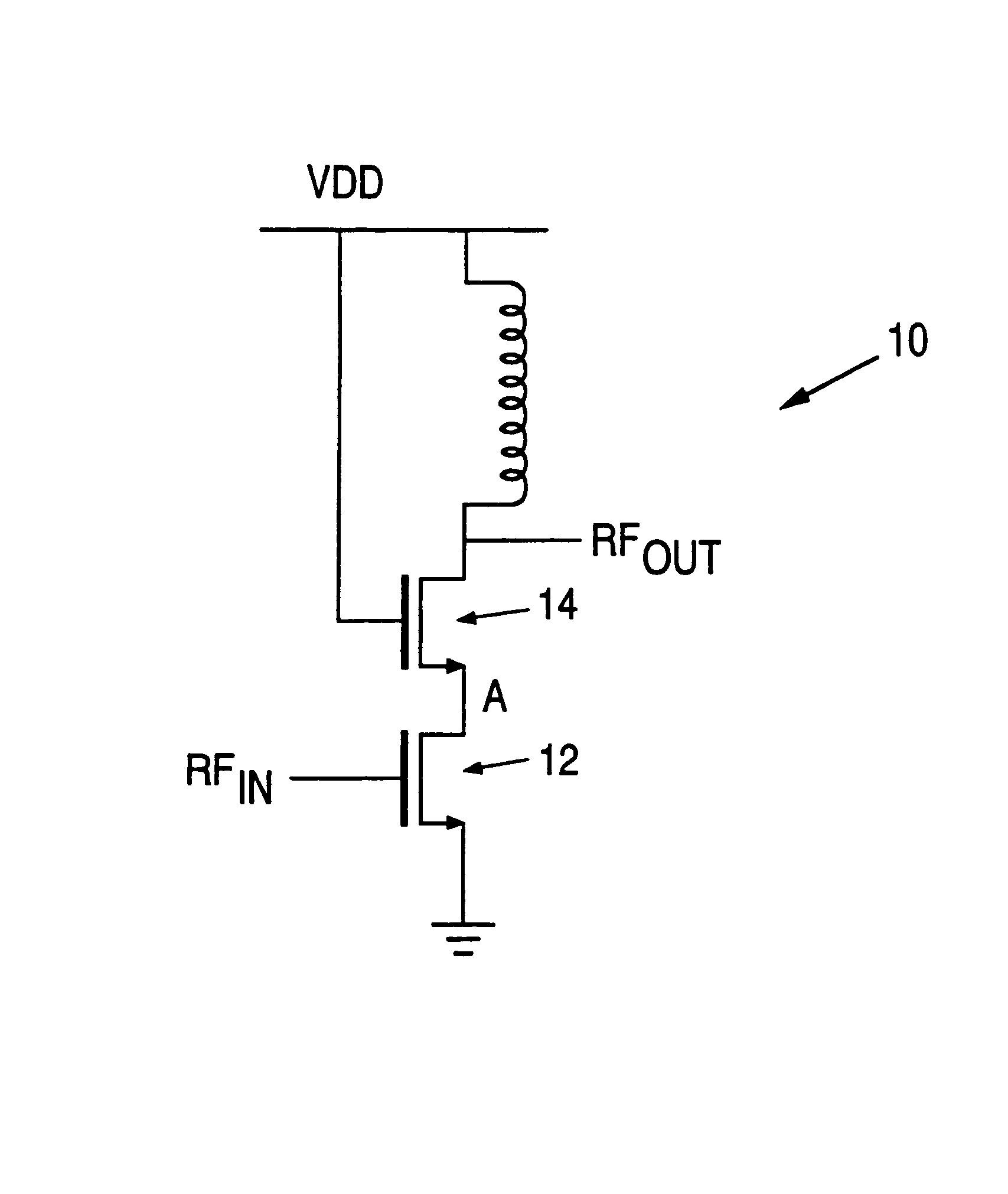
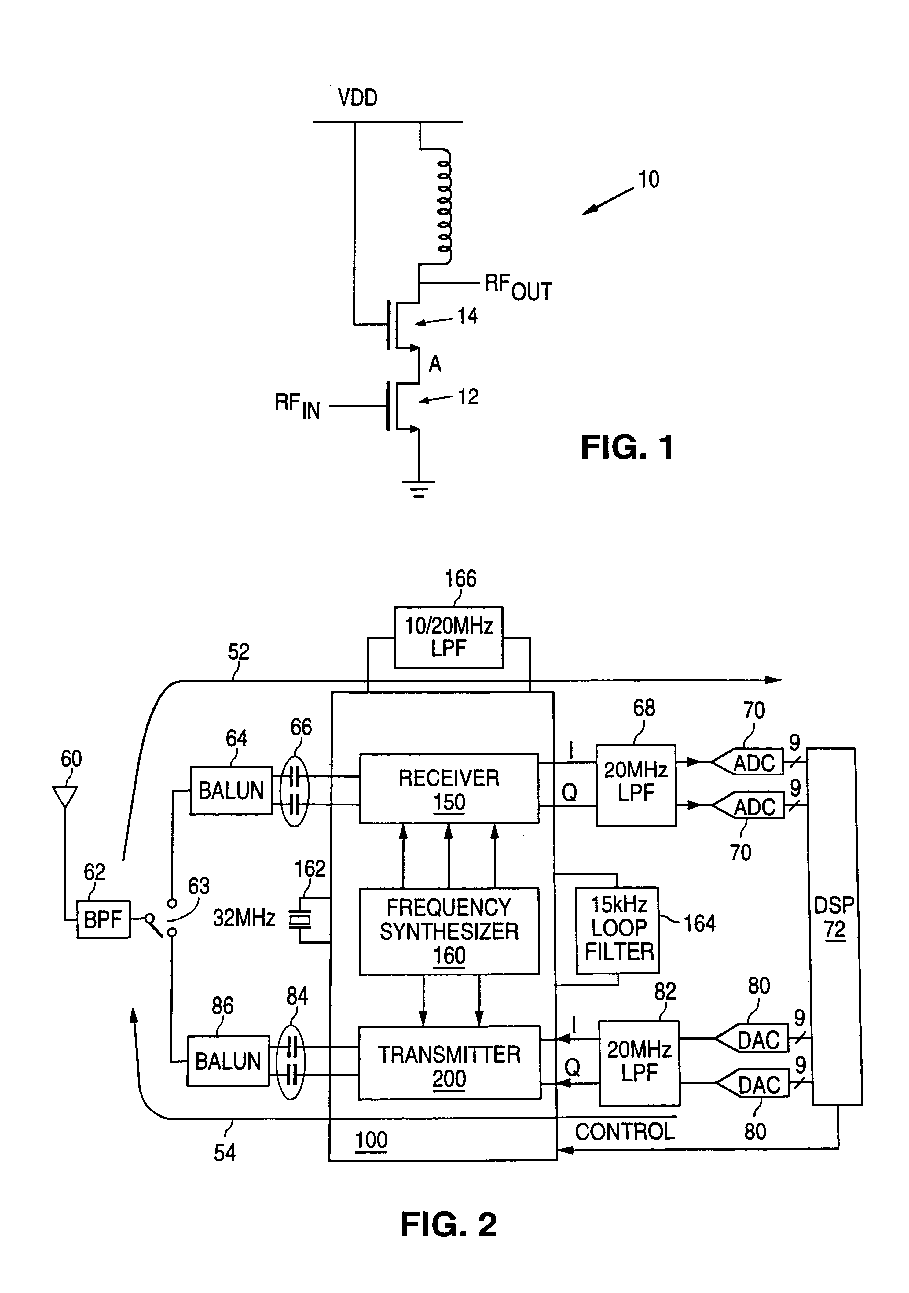
FIG. 1 illustrates a breakdown resistant transistor structure 10, which is one aspect of the present invention and is used in the final output stage of a power amplifier that is intended to be integrated with other CMOS circuit components, as described further hereinafter. The basic topology of this output stage is two NMOS transistors 12 and 14. As illustrated, a communication signal, such as a electromagnetic signal and typically a radio frequency signal, described herein as radio frequency input signal Rfin, is input at the gate of transistor 10, and the gate of transistor 14 is connected to the power supply voltage Vdd. Transistor 12 provides the transconductance necessary for power-amplification, and transistor 14 protects transistor 12 from the high voltage swings that result on the RFout node. Since transistor 14 is connected such that it has a unity current gain, it does not significantly degrade the transconductance of transistor 12 and can tolerate voltage amplitudes at RF...
PUM
 Abstract
Description
Claims
Application Information