CMOS image sensor with substrate noise barrier

a noise barrier and image sensor technology, applied in the field of solid-state image sensors, can solve the problems of not being compatible with a standard cmos process, consuming a lot of power, and the signal generated from the direct measurement of the current from the photoelectric conversion typically has a poor signal to noise ratio (s/n), so as to prevent latching and reduce the distance between the micro lens and the corresponding photodiode.

Inactive Publication Date: 2005-02-08
GALAXYCORE SHANGHAI
View PDF5 Cites 35 Cited by
  • Summary
  • Abstract
  • Description
  • Claims
  • Application Information

AI Technical Summary

Benefits of technology

The present invention pertains to new designs of CMOS Image sensors. According to one aspect of the present invention, the substrate traditionally used in the CMOS process is a same doping type of an EPI layer and replaced by a substrate that is of different doping type of the EPI layer, leading to layers on top of each other. When two different voltages are applied respectively to the two layers, a reversely biased junction is formed between the two layers so as to form a potential barrier under a photo diode. The potential barrier prevents noise electrons diffusing from a substrate layer (e.g., the lower one of the two layers) to the photo diode. According to another aspect of the present invention, a deep well with the same type of the EPI layer is implanted in the EPI layer to prevent latch-up between wells and the substrate. According to still another aspect of the present invention, the distance between a micro lens and a corresponding photodiode is reduced by adding an extra CMP step after a last oxide layer deposition.
One of the objects in the present invention is to provide improved designs on CMOS image sensors with low substrate diffusing noise and reduced distance between micro-lenses and photo diodes.

Problems solved by technology

However, the signal generated from the direct measurement of the current from the photoelectric conversion typically has a poor signal to noise (S / N) ratio.
A CCD device uses complicated driving signals of large voltage swings, and thus, consumes a lot of power.
A typical CCD fabrication process is optimized for charge transfer; and it is not compatible with a standard CMOS process.
Thus, a CCD image sensor is difficult to be integrated with signal processing circuitry, which is typically implemented by Complementary Metal-Oxide Semiconductor (CMOS) circuitry, and thus, difficult to be implemented in a wider variety of applications.
The first disadvantage is that poor MTF (modulate transfer function) and high noise caused by charge diffusion in substrate field-free region.
Some of the electrons / hole pairs will be recombined in the substrate However, there are still a significant amount of electrons that will be diffused to the neighbor photo diodes and cause poor MTF and high noise.
The second disadvantage is the large distance between the micro-lens 138 to the photo-sensitive silicon region (N well 108 / P−EPI 104).
This large distance will lower the sensor sensitivity and cause the optical cross talk problems between sensor pixels.

Method used


Image

  • CMOS image sensor with substrate noise barrier
  • CMOS image sensor with substrate noise barrier
  • CMOS image sensor with substrate noise barrier

Examples


Embodiment Construction

Embodiments of the invention are discussed herein with reference to FIGS. 2-6. However, those skilled in the art will readily appreciate that the detailed description given herein with respect to these figures is for explanatory purposes as the invention extends beyond these limited embodiments.

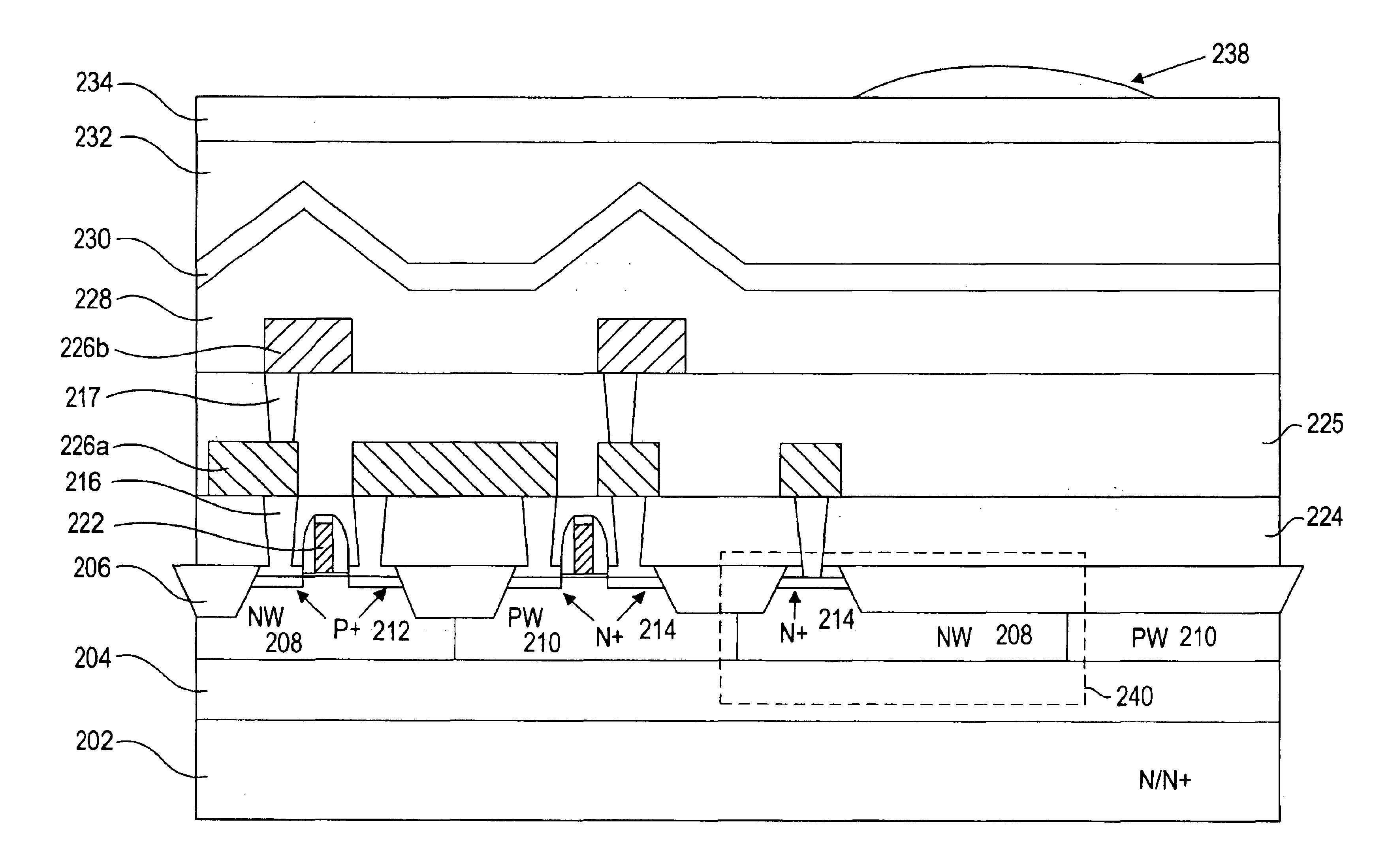
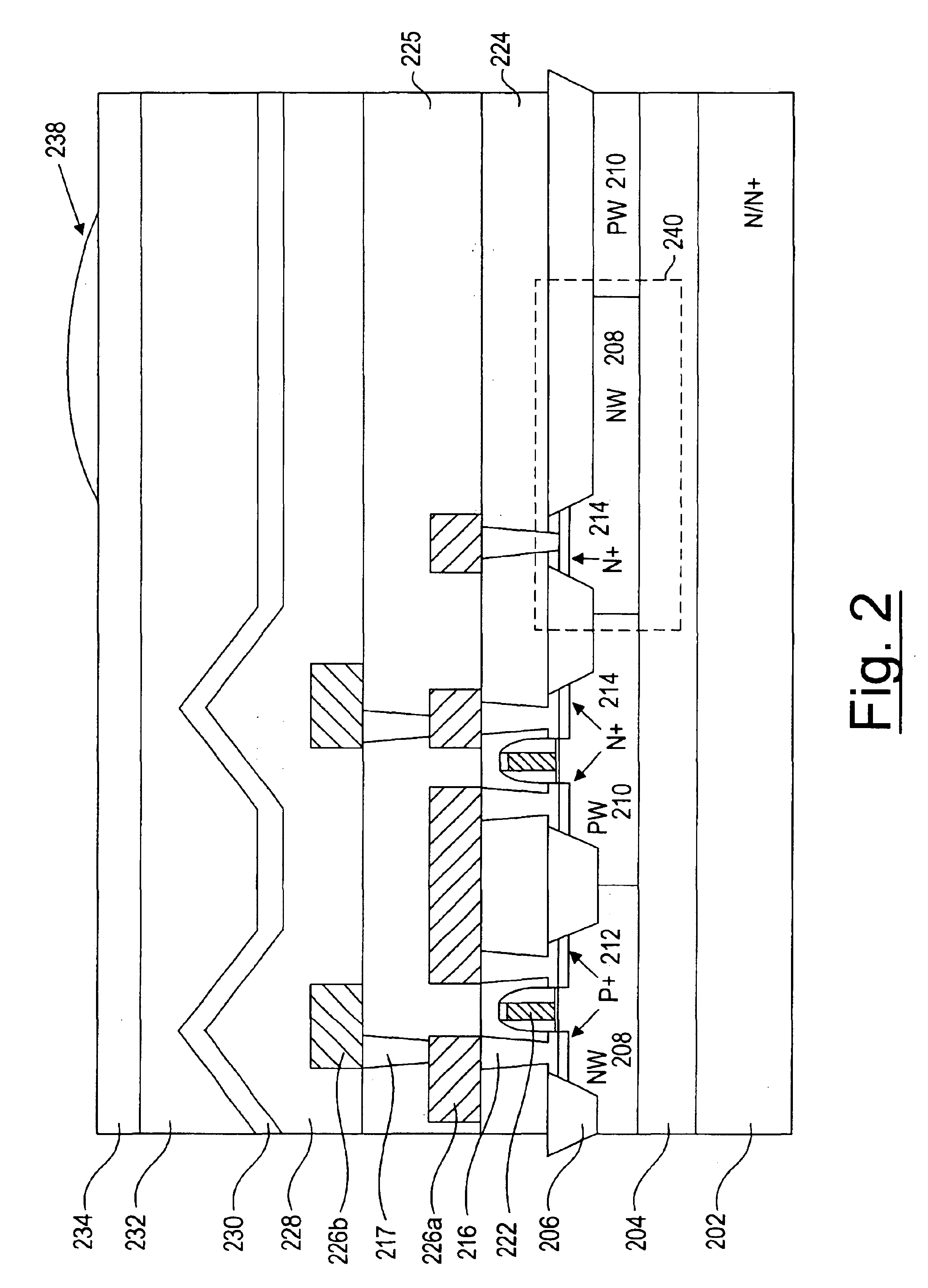
Referring now to FIG. 2, a CMOS image sensor according to one embodiment of the present invention is shown. Unlike the conventional CMOS image sensor, a CMOS image sensor according to one embodiment of the present invention includes an N or N+ type substrate layer 202, in contrast to a conventional P+ substrate.

A P− type Epi layer on top of an N / N+ type substrate 202 is connected to the ground and N / N+ type substrate 202 is connected to certain high voltage e.g., 2V. A depletion layer is formed between the interface P−Epi layer 204 to the N / N+ substrate 202. This depletion layer minimizes the P−EPI field-free region which is just under the photo diode depletion part also prevents photo genera...


PUM


Abstract

An image sensor element includes a vertical overflow drain structure to eliminate substrate charge diffusion causing CMOS image sensor noise. An extra chemical mechanical polish step used to shorten the micro-lens to silicon surface distance in order to reduce optical cross talking. One embodiment uses N type substrate material with P− epitaxial layer to form a vertical overflow drain. Deep P well implantation is introduced to the standard CMOS process to prevent latch-up between an N well to an N type substrate. A photo diode is realized by stacked N well / Deep N well and stacked P well / Deep P well to improve performance.

Description

FIELD OF THE TECHNOLOGYEmbodiments of the present invention relate to semiconductor devices, and more specifically to a solid-state image sensor.BACKGROUNDImage sensors can be used in a variety of applications, such as digital still cameras, PC cameras, digital camcorders and Personal Communication Systems (PCS), as well as analog and digital TV and video systems, video game machines, security cameras and micro cameras for medical treatment. With the development of the telecommunication and computer system, the demand for image sensors will be much more increased.An image sensor cell typically has a photodiode element that is capable of converting light (e.g., visible light, infrared light and ultraviolet light) into electric signals. When photons are absorbed, electron-hole pairs are created through photoelectric conversion. A depletion region is formed in a photodiode when the photodiode is reverse-biased. The electric field in the depletion region separates the electron-hole pair...

Claims


Application Information

Patent Timeline
Patent Type & Authority Patents(United States)
IPC IPC(8): H01L21/00H01L21/70H01L21/8238H01L27/146
CPCH01L27/14632H01L27/14601H01L27/146
Inventor ZHAO, LIXIN
Owner GALAXYCORE SHANGHAI
Why Eureka
Try Eureka