Component and antennae assembly in radio frequency identification devices

a technology of radio frequency identification and components, applied in the direction of printed circuit manufacturing, printed element electric connection formation, instruments, etc., can solve the problem of dramatic increase in the manufacturing cost of rfid devices, and achieve the effect of facilitating the production of smart cards and smart inlays and enhancing electrical components

Inactive Publication Date: 2005-02-08
NANOPIERCE TECH
View PDF65 Cites 238 Cited by
  • Summary
  • Abstract
  • Description
  • Claims
  • Application Information

AI Technical Summary

Benefits of technology

Similarly, the production of smart cards and smart inlays can be facilitated in another aspect of the invention wherein an electrical component is enhanced by particles simultaneously with a plurality of other electronic components in an array. Such an array bay be either one or two dimensional. Each of the plurality of electrical components has at least one electrical contact site. In this embodiment, the hard particles are applied to the contact sites, such that at least one hard particle is affixed to each of the ele

Problems solved by technology

For these conventional methods, the use of high temperatures, expensive materials, or expensive high precis

Method used


Image

  • Component and antennae assembly in radio frequency identification devices
  • Component and antennae assembly in radio frequency identification devices
  • Component and antennae assembly in radio frequency identification devices

Examples


first embodiment

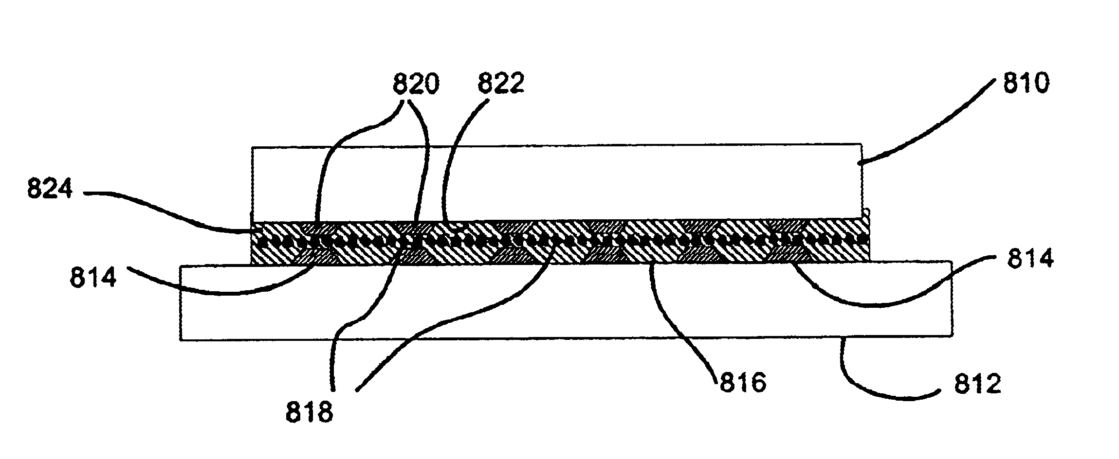
FIG. 12A depicts conducting area 1228 of a coil antenna structure on a smart inlay base 1225. The number of coil windings of the conducting area 1228 is dependant on the are of the smart inlay substrate 1218 and the requirements of the particular chip used. The conducting area may be made, for example, of copper, aluminum, silver, gold, and carbon, and applied to the substrate, for example, by screen printing a metal paste or etching a foil laminate layer. The substrate material 1218 may be paper or plastic foil made, for example, of polyvinyl chloride (PVC), polyethylene (PET), and polypropylene. Antenna contacts 1228a and 1228b are provided on the top of substrate 1218 for placement of a chip as described with reference to FIGS. 11A-11D. A bridge 1228c on the bottom side of the substrate 1218 provides an electrical connection through apertures in the substrate 1218 between antenna contact 1228b and the end of the conducting area 1228 opposite the end of the conducting area 1228 at...

second embodiment

FIG. 12B depicts a conducting area 1228 designed as a multiple coil antenna in a smart inlay 1230b. In this embodiment there is no bridge and the chip 1200 is positioned over the windings of the conductive area 1228 to connect to antenna contacts 1228a and 1228b connecting the ends of one or more of the coils as discussed above with reference to FIGS. 11A-11D. Also the conductive area 1228 is only on one side of the substrate 1218.

third embodiment

FIG. 12C depicts a conducting area 1228 for a smart inlay 1230c. The conducting area consists of a first rectangular conducting area 1228a and a second 1228b rectangular conducting area extending from each side of the chip 1200 along the length of the substrate 1218 of the smart inlay 1230c. The chip 1200 electrically connects with both first rectangular area 1228a and second rectangular area 1228b by its particle-enhanced bond pads as described in FIGS. 11A-11D. This design of conducting areas 1228a and 12228b is, for example, of a high frequency antenna.


PUM


Abstract

Permanent physical and electrical attachment of electrically conductive contacts of a first component in a RFID device, such as a smart card or smart inlay, is made to the electrically conductive contacts of a second component of the device, for example, a conductive area, such as an antenna. Attachment is achieved by co-depositing metal and electrically conductive hard particles upon the conductive contacts of either the first or second components and then using a non-conductive adhesive to provide permanent bond between the components and their conductive contacts.

Description

FIELD OF THE INVENTIONThe invention relates broadly to methods and configurations for electrical and mechanical connection of semiconductor radio frequency transceiver chips to antenna structures and particularly to radio frequency identification device assemblies and methods for fabrication thereof.BACKGROUND OF THE INVENTIONA radio frequency identification device (“RFID”) by definition is an automatic identification and data capture system comprising readers and tags. Data is transferred using electric fields or modulated inductive or radiating electromagnetic carriers. RFID devices are becoming more prevalent in such configurations as, for example, smart cards, smart labels, security badges, and live stock tags.Typically, a smart card is a flexible, credit card size, plastic device embedded with a chip that provides memory, microprocessing capability, and RF transmission and reception (a “transceiver”). When employed with a “reader,” operating power is supplied to the chip and th...

Claims


Application Information

Patent Timeline
IPC IPC(8): H01L21/56H01L21/02H01L21/60H01L23/48H01L23/498H01L23/485H05K3/40H05K3/32G06K19/07G06K19/077
CPCG06K19/07752H01L21/563H01L23/49811H01L24/10H01L24/29H01L24/31H01L24/48H01L24/83H05K3/325H05K3/4007H01L24/95H01L24/13H01L2224/0401H01L2224/05599H01L2224/13099H01L2224/13109H01L2224/13609H01L2224/16225H01L2224/29409H01L2224/48091H01L2224/48227H01L2224/48228H01L2224/48465H01L2224/73203H01L2224/73204H01L2224/7565H01L2224/83101H01L2224/83191H01L2224/83192H01L2224/838H01L2924/01003H01L2924/01004H01L2924/01005H01L2924/01006H01L2924/01011H01L2924/01012H01L2924/01013H01L2924/01014H01L2924/0102H01L2924/01022H01L2924/01025H01L2924/01027H01L2924/01028H01L2924/01029H01L2924/0103H01L2924/01031H01L2924/01032H01L2924/01033H01L2924/01038H01L2924/01039H01L2924/01046H01L2924/01047H01L2924/01049H01L2924/0105H01L2924/01051H01L2924/01056H01L2924/01057H01L2924/0106H01L2924/01075H01L2924/01078H01L2924/01079H01L2924/01082H01L2924/01083H01L2924/01322H01L2924/01327H01L2924/014H01L2924/0781H01L2924/14H01L2924/3011H01L2224/2919H01L2924/00014H01L2924/01019H01L2924/01023H01L2924/01024H01L2924/01037H01L2924/01044H01L2924/01045H01L2924/01055H01L2924/01068H01L2924/0665H01L2224/29101H01L2224/32225H01L2924/0132H01L2224/95085H01L2924/15724H01L2924/15747H01L2924/1579H01L2224/29111H01L2224/451H01L2924/10253H01L2224/2929H01L2224/293H01L2224/83851H01L2224/13019H01L2224/81193H01L2924/12041H01L2924/07811H01L2224/29499H01L2224/325H01L2924/07802H01L2924/00H01L2224/45099H01L2924/00012H01L2224/13H01L2924/181H01L23/48
Inventor NEUHAUS, HERBERT J.WERNLE, MICHAEL E.BLUM, FREDERICK A.KOBER, MICHAEL
Owner NANOPIERCE TECH
Why Eureka
Try Eureka