Transparent laminate, method for producing the same, and plasma display panel

a technology of transparent laminate and plasma display panel, which is applied in the direction of identification means, instruments, lighting and heating apparatus, etc., can solve the problems of insufficient electromagnetic wave shielding function, difficult continuous structure, and reduced transmittance in a certain wave range, so as to achieve good visibility and reduce the effect of transmittance dependen

Inactive Publication Date: 2005-02-15
NITTO DENKO CORP
View PDF14 Cites 44 Cited by
  • Summary
  • Abstract
  • Description
  • Claims
  • Application Information

AI Technical Summary

Benefits of technology

Upon such circumstances, an object of the present invention is to provide a transparent laminate which can satisfy all properties such as electromagnetic wave shielding property, near-infrared cutting property, visible light transmitting property and visible light low-reflecting property required of a PDP filter in spite of a relatively simple structure of the transparent laminate and which can exhibit a color tone of neutral gray with little dependence of the transmittance of the transparent laminate on wavelengths in a visible light range without use of any absorbent such as dyes, or the like. Another object of the present invention is to provide a light-weight thin PDP filter of good visibility using the transparent laminate.

Problems solved by technology

As a result, each of the islands is shaped like a sphere, so that it is difficult to form a continuous structure even in the case where the thickness of the thin film is relatively large.
Particularly in the case of a silver transparent conductive thin film, the electromagnetic wave shielding function cannot be fulfilled sufficiently because electric resistance in the direction of width of the film is reduced remarkably as well as visible light transmittance in a certain wave range is reduced greatly by surface plasma resonance absorption.

Method used


Image

  • Transparent laminate, method for producing the same, and plasma display panel
  • Transparent laminate, method for producing the same, and plasma display panel

Examples


example 1

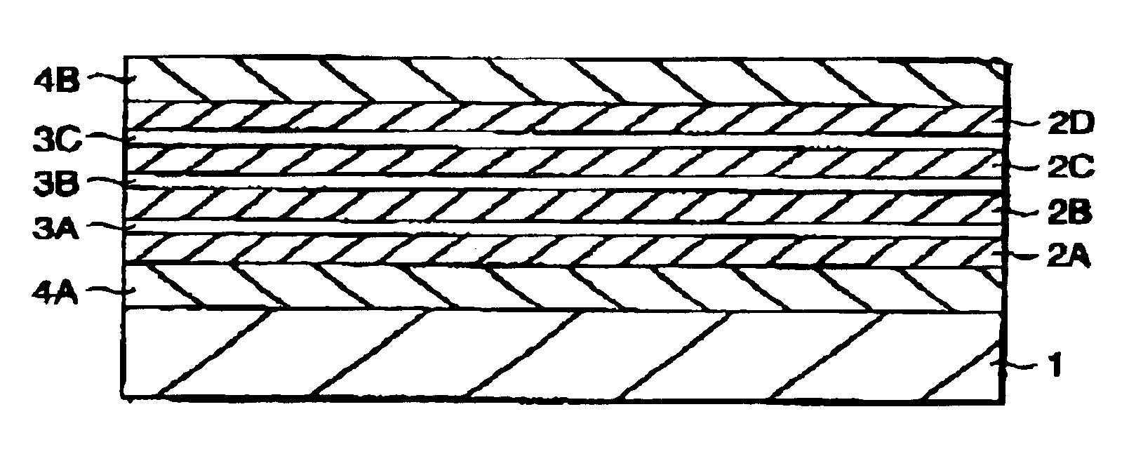
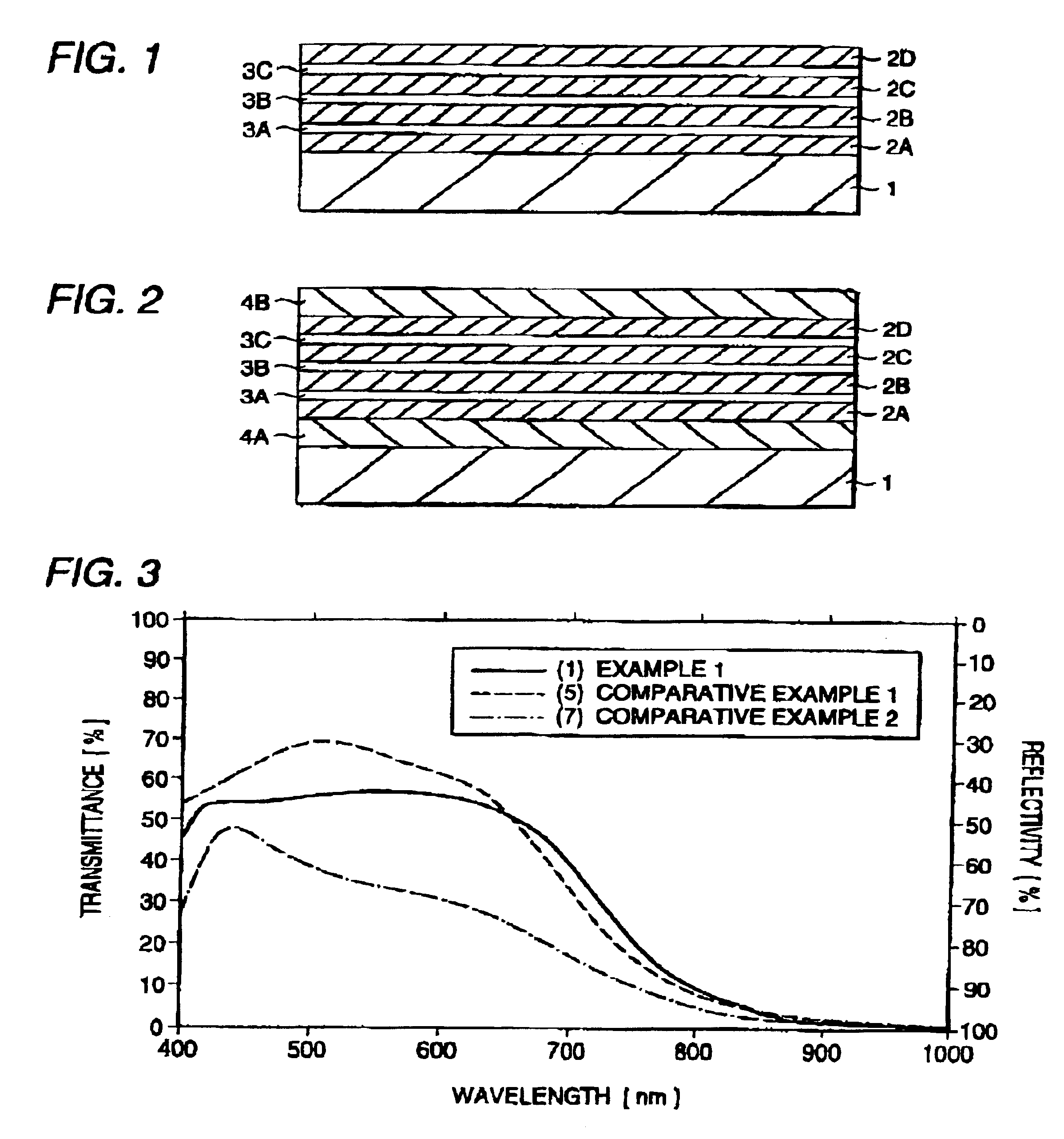
Three thin-film units each unit consisting of a combination of a high-refractive-index transparent thin film and a silver transparent conductive thin film were deposited successively on one side of a 125 μm-thick transparent polyethylene terephthalate (hereinafter referred to as “PET”) film by a DC magnetron sputtering method. A high-refractive-index transparent thin film was further deposited on a surface of the laminate of the three thin-film units. Thus, a transparent laminate was produced by the aforementioned method. In this occasion, In2O3 containing 12.6% by weight of TiO2 (hereinafter abbreviated as “IT”) was used as a target material for depositing the high-refractive-index transparent thin films and Ag containing 5% by weight of Au (hereinafter abbreviated as “Ag”) was used as a target material for depositing the silver transparent conductive thin films.

Film thickness was controlled by use of the analytical curve of the deposition rate obtained on the basis of film thickne...

example 2

An SiO2 layer was deposited on a 125 μm-thick transparent PET film at room temperature by a vacuum vapor deposition method. The refractive index nL of SiO2 measured by an ellipsometer was 1. 45. The thickness of the SiO2 layer was set to be 95 nm. Three thin-film units each consisting of a combination of an IT thin film and an Ag thin film were deposited successively on a surface of the SiO2 layer in the same manner as in Example 1. An IT thin film was further deposited on a surface of the laminate of the three thin-film units. Thus, a transparent laminate was produced as a sample (9). The thicknesses of respective thin films were as shown in numerical values (unit: nm) put in the following parentheses. The roll temperature for depositing the IT thin films and the Ag thin films and the deposition rate of Ag were as follows.

Sample (9)

PET / SiO2(95) / IT(32.5) / Ag(13) / IT(65) / Ag(13) / IT(65) / Ag(13) / IT(32.5)

<Roll Temperature: 373 K, deposition rate of Ag: 1.8 nm / sec>

example 3

In the transparent laminate produced in Example 2, an SiO2 layer was deposited on a surface of the IT thin film located as the outermost layer at room temperature by a vacuum vapor deposition method so that the thickness of the SiO2 layer was set to be 190 nm. Thus, a transparent laminate was produced as a sample (10). The thicknesses of respective thin films were as shown in numerical values (unit: nm) put in the following parentheses.

Sample (10)

PET / SiO2(95) / IT(32.5) / Ag(13) / IT(65) / Ag(13) / IT(65) / Ag(13) / IT(32.5) / SiO2(190)


PUM

PropertyMeasurementUnit
thicknessaaaaaaaaaa
thicknessaaaaaaaaaa
thicknessaaaaaaaaaa

Abstract

In a transparent laminate, n thin-film units (n=3 or 4) are laminated unit by unit successively on a surface of a substrate, and a high-refractive-index transparent thin film is deposited on a surface of the laminate of the n thin-film units, each of the n thin-film units consisting of a high-refractive-index thin film and a silver transparent conductive thin film. When the silver transparent conductive thin films are deposited by a vacuum dry process, the temperature T(K) of the transparent substrate at the time of film deposition is set to be in a range 340≦T≦410, whereby the transparent laminate having a standard deviation of visible light transmittance which is not larger than 5% in a wave range of from 450 to 650 nm can be produced.

Description

BACKGROUND OF THE INVENTION1. Field of the InventionThe present invention relates to a transparent laminate, a method for producing the transparent laminate, and a plasma display panel (hereinafter referred to as “PDP”) filter using the transparent laminate.The present application is based on Japanese Patent Applications No. Hei. 11-369355 and 2000-383072, which are incorporated herein by reference.2. Description of the Related ArtNowadays in the society where information orientation is advancing remarkably, performance required of a display to be used as a terminal for displaying an image is diversified greatly. Especially, a great deal of attention has been paid to a PDP as a novel display succeeding a CRT and a liquid-crystal display because it is easy to increase the size of the PDP while reducing the thickness of the PDP. The PDP has already come onto the market.In the PDP, electric discharge is produced in rare gas enclosed in the panel, especially, in gas containing neon as a...

Claims


Application Information

Patent Timeline
Patent Type & Authority Patents(United States)
IPC IPC(8): G02B1/11G02B1/10G02B5/28B32B15/08C23C14/06G02B5/26G09F9/00
CPCG02B1/10G02B1/116H01J2211/44Y10T428/31678Y10T428/31692C23C14/00
Inventor NAKAMURA, TOSHITAKASASA, KAZUAKIHIEDA, YOSHIHIROMIYAUCHI, KAZUHIKO
Owner NITTO DENKO CORP
Why Eureka
Try Eureka