Method of forming self-aligned contact structure with locally etched gate conductive layer

a contact structure and local etching technology, applied in the direction of semiconductor devices, electrical equipment, semiconductor/solid-state device details, etc., can solve the problems of high resistance of metal and generated conductivity not high enough for a good conductive layer of mos devices, and achieve the effect of low resistan

Inactive Publication Date: 2005-02-15
PROMOS TECH INC
View PDF5 Cites 376 Cited by
  • Summary
  • Abstract
  • Description
  • Claims
  • Application Information

AI Technical Summary

Benefits of technology

The main object of the present invention is to provide methods of forming a self-aligned contact structure with a locally etched second conductive layer. The self-aligned contact structure formed by said methods can have a larger process window, l

Problems solved by technology

However, the disadvantage of the polysilicon material is that its resistance is higher than that of the metal.
Although the resistance can be reduced by doping impurities, the generated conductivity is not high enough for a g

Method used


Image

  • Method of forming self-aligned contact structure with locally etched gate conductive layer
  • Method of forming self-aligned contact structure with locally etched gate conductive layer
  • Method of forming self-aligned contact structure with locally etched gate conductive layer

Examples


first embodiment

the present invention is described by the structures from FIGS. 3A-3F and the method shown in the flow chart of FIGS. 4A-4B.

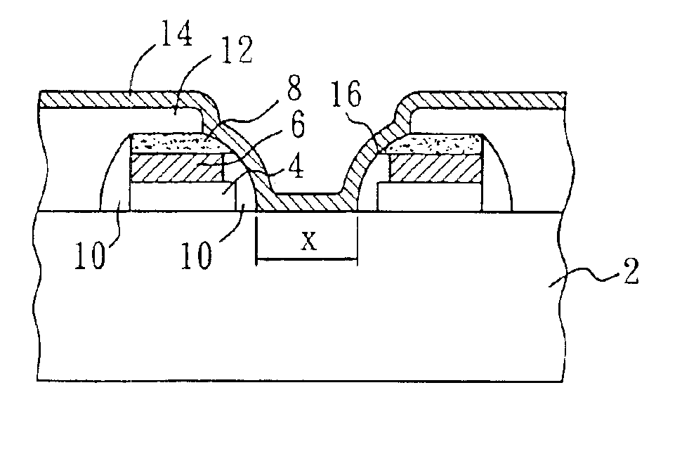
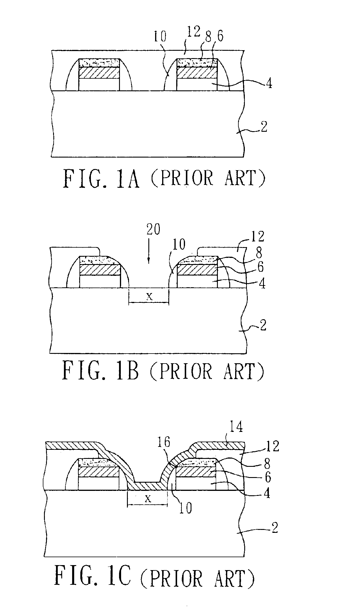
First, a substrate 2, which has a first conductive layer 4, a second conductive layer 6, and an insulating layer 8 formed in sequence from bottom to top, is prepared. The first conductive layer 4 can be a polysilicon layer or an amorphous silicon layer. The second conductive layer 6 can be a metal silicide layer, such as a tungsten silicide (WSi) layer, and the insulating layer 8 can be a silicon nitride layer. Next, as shown in FIG. 4A, a gate conductor (GC) photomask is opened (step 401). Next, a plurality of separated gate structures is formed by performing an etching process to the top surface of the substrate 2 (step 402).

Next, as shown in FIGS. 3A-4A, a photoresist material layer 22 is deposited, or an anti-reflective coating (ARC, not shown in the figures), and a photoresist material layer 22 are in turn deposited on the entire surface of the substrate 2...

second embodiment

the present invention is illustrated in the structures from FIGS. 5A-5F and the method shown in the flow chart of FIGS. 6A-6B.

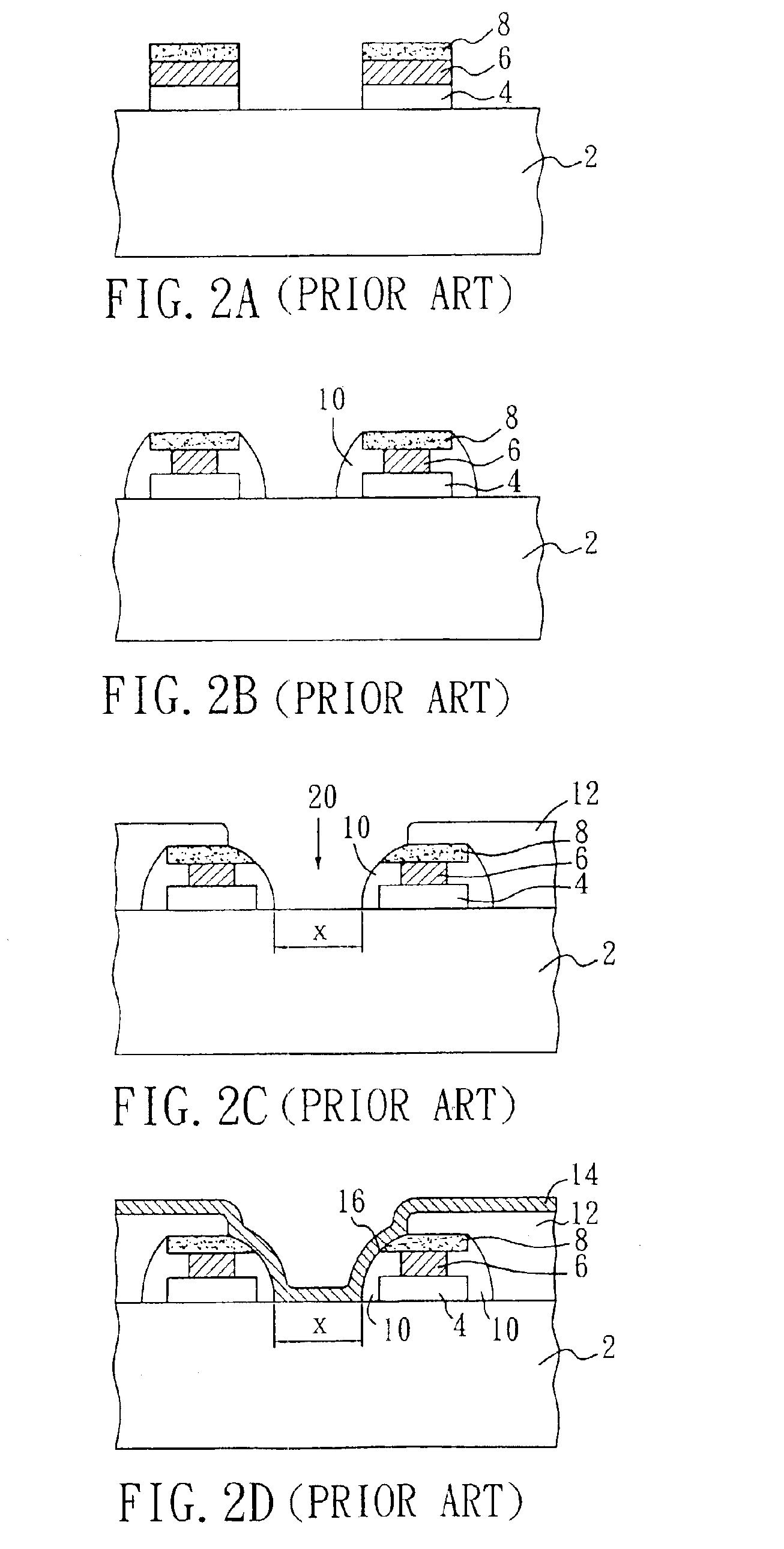
First, a substrate 2 that has a first conductive layer 4, a second conductive layer 6, and an insulating layer 8 formed in sequence from bottom to top, is prepared. The first conductive layer 4 can be a polysilicon layer or an amorphous silicon layer, the second conductive layer 6 can be a metal silicide layer, such as a tungsten silicide (WSi) layer, and the insulating layer can be a silicon nitride layer. Next, as shown in FIG. 5A, the gate conductor (GC) photomask is opened (step 601). Next, a plurality of separated gate structures is formed by performing an etching process to the top surface of the substrate 2 (step 602).

Next, as shown in FIGS. 5A-6A, a photoresist material layer 22 is deposited, or an anti-reflective coating (ARC, not shown in the figures) and a photoresist material layer 22 are deposited, in turn, on the entire surface of the substrate ...


PUM


Abstract

A method of forming a self-aligned contact structure with a locally etched conductive layer comprises the steps of: preparing a substrate formed with gate structures comprising a first conductive layer, a second conductive layer, and an insulating layer; depositing a photoresist material layer on the substrate; performing a lithographic step with a bit-line contact node photomask or a bit-line contact photomask to expose a portion of the surface of the substrate; etching the exposed second conductive layer with an etchant; removing the remaining photoresist material layer; forming a sidewall spacer on the sidewalls of each gate structure; forming a dielectric layer to cover the substrate; and performing lithographic and etching steps to remove the dielectric layer and to form self-aligned contact structure.

Description

FIELD OF THE INVENTIONThe present invention relates to a method of forming a self-aligned contact structure and, in particular, the present invention relates to a method of eliminating the disadvantage of the short circuit problem of a gate conductor / bit-line contact (GC / CB) formed in prior manufacturing processes and increasing a larger process window.BACKGROUND OF THE INVENTIONNormally, a metal oxide semiconductor (MOS) device is composed of a metal layer, a silicon oxide layer, and a substrate. Since the adhesion between the metal and the oxide is poor, a polysilicon material is often used to replace the metal so as to form the conductive layer of an MOS device. However, the disadvantage of the polysilicon material is that its resistance is higher than that of the metal. Although the resistance can be reduced by doping impurities, the generated conductivity is not high enough for a good conductive layer of an MOS device. A general solution is to add a metal silicide layer on the ...

Claims


Application Information

Patent Timeline
IPC IPC(8): H01L23/48H01L23/485H01L21/336H01L21/60
CPCH01L21/76897H01L23/485H01L29/66659H01L2924/0002H01L2924/00
Inventor TUNG, MING-SHENGLEE, YUEH-CHUAN
Owner PROMOS TECH INC
Why Eureka
Try Eureka