

Relaxed SiGe layers on Si or silicon-on-insulator substrates by ion implantation and thermal annealing
a technology of si or silicon-on-insulator substrate and ion implantation, which is applied in the direction of basic electric elements, electrical apparatus, semiconductor devices, etc., can solve the problems of high threading dislocation density, inhomogeneous distribution of threading dislocations over the whole wafer surface, and deleterious effects on the properties of electronic and optoelectronic devices
- Summary
- Abstract
- Description
- Claims
- Application Information
AI Technical Summary
Benefits of technology
Problems solved by technology
Method used
Image

Examples
example 1
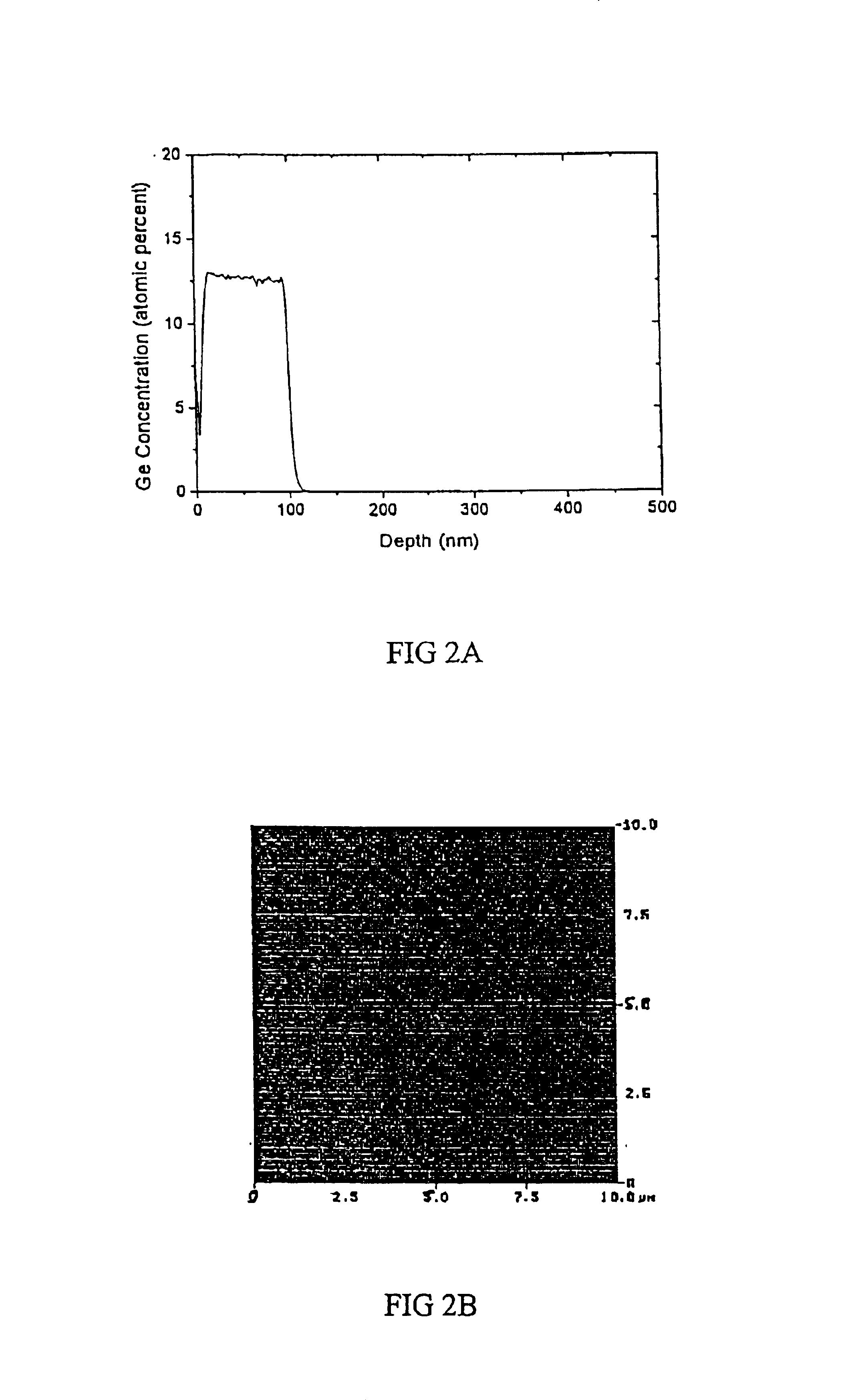
[0111]In this example, a “virtual substrate” was fabricated by depositing a 100 nm thick pseudomorphic Si0.85Ge0.15 layer on a bulk Si substrate. The resultant structure was then implanted with He+ at a dose of about 1×1016 cm−2, using an implant energy of about 21 keV. The structure was subsequently annealed at approximately 850° C. for about 1 hour. HRXRD measurements after annealing show that 41% of the lattice mismatch strain was relieved. The sample had an RMS surface roughness of about 0.29 nm and an etch pit (TD) density of about 1×105 cm−2.
example 2
[0112]A second implementation of the inventive process was also done according to the structure of FIG. 6, where layers 5 and 10 are a bulk Si substrate and layer 40 is a 100 nm thick pseudomorphic Si0.85Ge0.15 layer as measured by HRXRD prior to ion implantation. He+ was implanted at a dose of about 1×1016 cm−2, using an implant energy of about 21 keV. The wafer was subsequently annealed at approximately 850 ° C. for about 30 min. The SiGe layer was about 38% relaxed.
example 3
[0113]A third implementation of the inventive process was also done according to the structure of FIG. 6, where layers 5 and 10 are a bulk Si substrate and layer 40 is an 188 nmthick Si0.79Ge0.21 pseudomorphic layer as measured by HRXRD prior to ion implantation. He+ was implanted at a dose of about 0.8×1016 cm−2 and at an energy of about 31 keV. The wafer was subsequently annealed at approximately 850° C. for about 1 hour. The SiGe layer was 69% relaxed. The RMS surface roughness was about 0.47 nm, and the etch pit (TD) density was about 2.7×105 cm2.
PUM
 Abstract
Description
Claims
Application Information