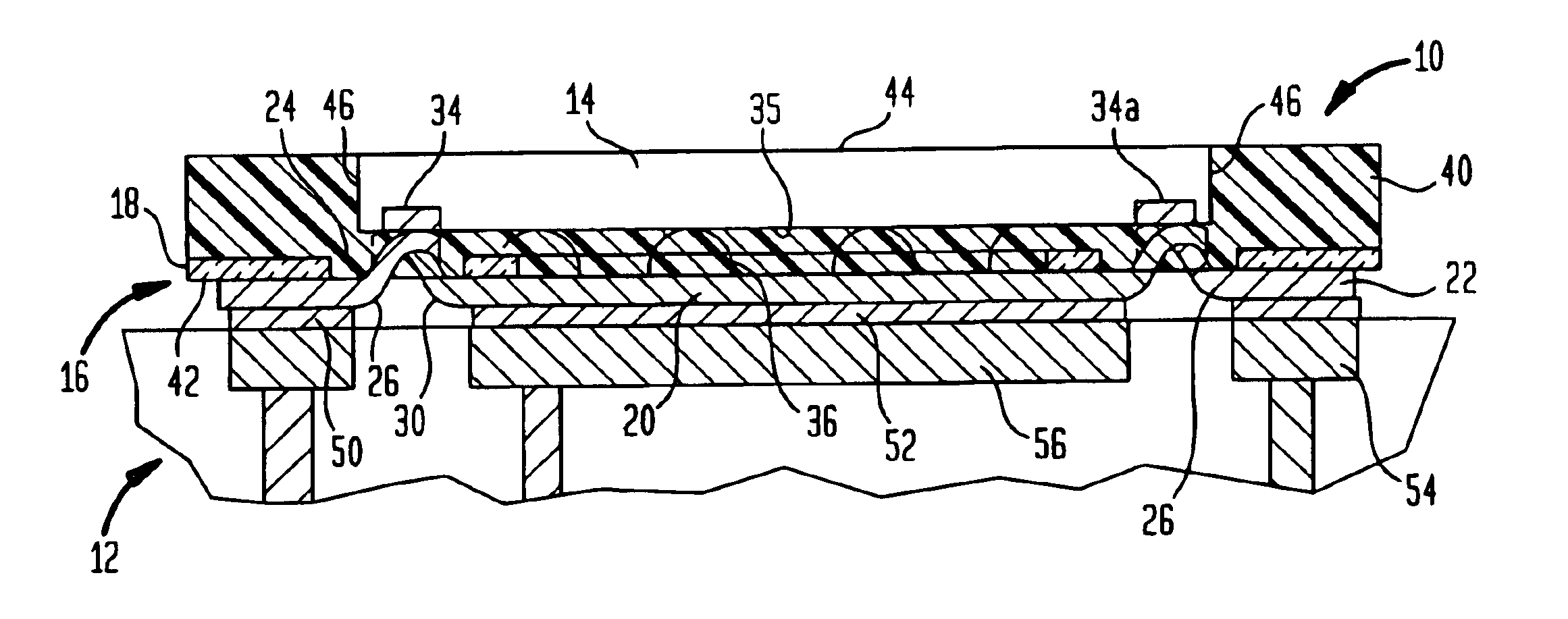
In certain embodiments, the packaged chip may include a metallic
heat spreader or “can” having a main or top wall structure overlying the rear surface of the chip so that a portion of the
heat spreader faces upwardly, away from the circuit panel when the packaged chip is assembled to the circuit panel. The
heat spreader desirably has a side wall projecting from the main portion of the heat spreader towards the front surface of the die. This wall desirably terminates in a horizontal surface or
flange. In the
assembly, the horizontal surface or
flange of the heat spreader desirably is metallurgically bonded to a spreader mounting on the circuit panel. The spreader facilitates
heat transfer from the packaged chip into the surroundings, away from the circuit panel. Where the spreader is bonded to the circuit panel, the spreader can also facilitate transfer of heat from the packaged chip into the circuit panel. The spreader can also serve as an RF shield, as a ground connection to the rear surface of the chip, or both. In an alternative arrangement, the side wall structure is bonded to a metallic feature on the
chip carrier, which in turn is bonded to a
mating feature of the circuit panel.
A further aspect of the invention provides a packaged
semiconductor chip. The packaged chip according to this aspect of the invention desirably includes a first
semiconductor chip having an upwardly-facing front face, a downwardly-facing rear face, edges bounding said faces and contacts exposed at said front surface, said first
semiconductor chip including
active components. A connecting element including passive components such as resistors and capacitors is electrically connected to at least some of the contacts of the first chip. The connecting element overlies the front face of the first chip and projects outwardly beyond the edges of the first chip. A
chip carrier is disposed below the rear surface of the first chip. The chip carrier has a bottom surface facing downwardly away from the first chip and has a plurality of terminals exposed at the bottom surface, at least some of such terminals being electrically connected to at least some of the contacts of the first chip through said connecting element. Most preferably, the connecting element is a second chip incorporating the passive elements, also referred to as a “passive chip.” The chip carrier may include a thermal conductor as discussed above, and may also include a spreader or
enclosure having a top wall overlying the rear surface of the connecting element or passive chip. As discussed above, these features provide further enhanced
thermal dissipation and
electromagnetic shielding.
A further aspect of the invention provides a packaged
surface acoustic wave or “SAW” device. The packaged device according to this aspect of the invention includes a SAW chip having an acoustically active region on its front surface. The SAW chip desirably is mounted front-face-down on a chip carrier having an inner surface and an outer surface so that the active region of the SAW chip front surface is aligned with a hole in the chip carrier. The front surface is sealingly connected to the chip carrier around the periphery of the hole, so that the active region of the SAW chip is maintained free of encapsulants and contaminants. Preferred structures according to this aspect of the invention can provide a thin, surface-mountable packaged
SAW device at low cost.
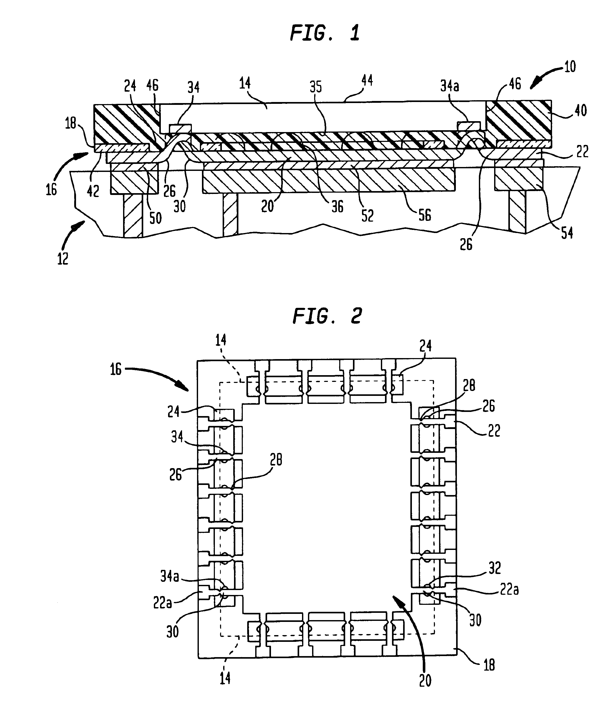
Yet another aspect of the invention provides A packaged semiconductor chip
assembly including a first semiconductor chip incorporating one or more
active components together with a passive chip incorporating one or more passive components selected from the group consisting of resistors and capacitors. The packaged chip according to this aspect of the invention also includes a chip carrier having terminals thereon. The chips are secured to said chip carrier, and at least some of said terminals being connected to at least one of said chips. The packaged chip according to this aspect of the invention desirably includes at least one
inductor defined at least in part by features on said chip carrier, said at least one
inductor being connected to at least one of said chips. As further explained below, the use of a passive chip to provide at least some of the resistors and capacitors affords significant savings in space and cost as compared to the use of discrete passive components, whereas formation of the
inductor at least in part on the chip carrier allows the use of thick, low-resistance windings in the inductor to provide inductors with a high quality factor or “Q.” The structural features of the foregoing aspects of the invention can be combined with one another or used separately.
Additional aspects of the invention provide methods of mounting chips to circuit panels. Methods according to this aspect of the invention desirably use packaged chips or modules and circuit panels as discussed above. In a method according to this aspect of the invention, the terminals are bonded to the contact pads and the thermal conductor is bonded to the thermal conductor mounting in a single operation. Most preferably, the terminals and thermal conductor are soldered or otherwise metallurgically bonded to the contact pads and to the thermal conductor mounting. Preferably, the contact pads and the thermal conductor carry
layers of solder before the packaged chip is assembled to the circuit panel. Alternatively, the solder may be provided on the contact pads and on the thermal conductor mounting of the circuit panel. In either case, the solder connections can be relatively thin
layers of solder as, for example, 25-50 microns thick. Stated another way, the connection between the packaged chip and the circuit panel may be a “
land grid array” rather than a
ball grid array. The ability to use thin solder connections further enhances the
electrical performance of the completed
assembly, and minimizes the height of the assembly. Moreover, there is typically no need for a layer of dielectric material or “underfill” surrounding the solder connections between the connection component and the circuit panel. This simplifies the connection procedure. Where a heat spreader is to be bonded to a spreader mounting on the circuit board, the spreader desirably is provided in place on the chip
package before the chip
package is assembled to the circuit panel, and the spreader is bonded to the circuit panel in the same bonding operation used to bond the terminals and thermal conductor.

