Method and apparatus for fabricating self-assembling microstructures

a microstructure and self-assembling technology, applied in the field of electromechanical integrated circuits, can solve the problems of inefficient use of precious die area, inability to realize the effect of reducing the cost of processing, and requiring special techniques, chemicals, equipment,

Inactive Publication Date: 2005-03-08
RGT UNIV OF CALIFORNIA
View PDF138 Cites 234 Cited by
  • Summary
  • Abstract
  • Description
  • Claims
  • Application Information

AI Technical Summary

Problems solved by technology

However, in the fabrication of gallium arsenide devices, substantial regions of a gallium arsenide wafer are typically unused and wasted.
Such unused regions generally create an inefficient use of precious die area.
In addition, processing gallium arsenide typically requires special techniques, chemicals, and equipment, and is therefore costly.
Methods such as flip chip bonding, lift off methods, and others, generally require large areas of a substrate and are incompatible with a micron sized state-of-art microstructure.
Such methods often create difficulty in positioning a particle onto a substrate.
This approach becomes limiting because the lattice structure of gallium arsenide mismatches that of silicon.
In addition, growing gallium arsenide onto silicon is inherently difficult and therefore costly.
Accordingly, gallium arsenide can not efficiently be grown on a silicon substrate.
However, severe limitations exist on the shape, size, and distribution of the components.
Furthermore, the structures disclosed by Yando typically possess millimeter sized dimensions and are therefore generally incompatible with micron sized integrated circuit structures.
Accordingly, the method and structure disclosed by Yando is thereby too large and complicated to be effective for assembling a state-of-art microstructure or component onto a substrate.
Such process is limiting because of the need for the human or robotics arm.
The human or robotics arm assembles each packaged device onto the substrate one-by-one and not simultaneously, thereby limiting the efficiency and effectiveness of the operation.
Moreover, the method uses centimeter sized devices (or packed surface mount integrated circuits), and would have little applicability with micron sized integrated circuits in die form.
A limitation to the method includes an apparatus capable of vibrating the structures, or an apparatus for pulsating air through the apertures.
Moreover, the method described relies upon centimeter-sized dies and would have little applicability with state-of-art micron sized structures.
The method becomes limiting because of the need for a shaking apparatus for the electromagnetic shaking step.
Moreover, the method is solely in context to electrode pedestals and silicon wafers, thereby limiting the use of such method to these structures.
A limitation with such method includes providing an apparatus capable of vibrating particles with electrostatic forces.
Moreover, the method of Cohn creates damage to a portion of the integrated circuits by mechanically vibrating them against each other and is also generally ineffective.
Accordingly the method typically becomes incompatible with a state-of-art microstructure.

Method used


Image

  • Method and apparatus for fabricating self-assembling microstructures
  • Method and apparatus for fabricating self-assembling microstructures
  • Method and apparatus for fabricating self-assembling microstructures

Examples


examples

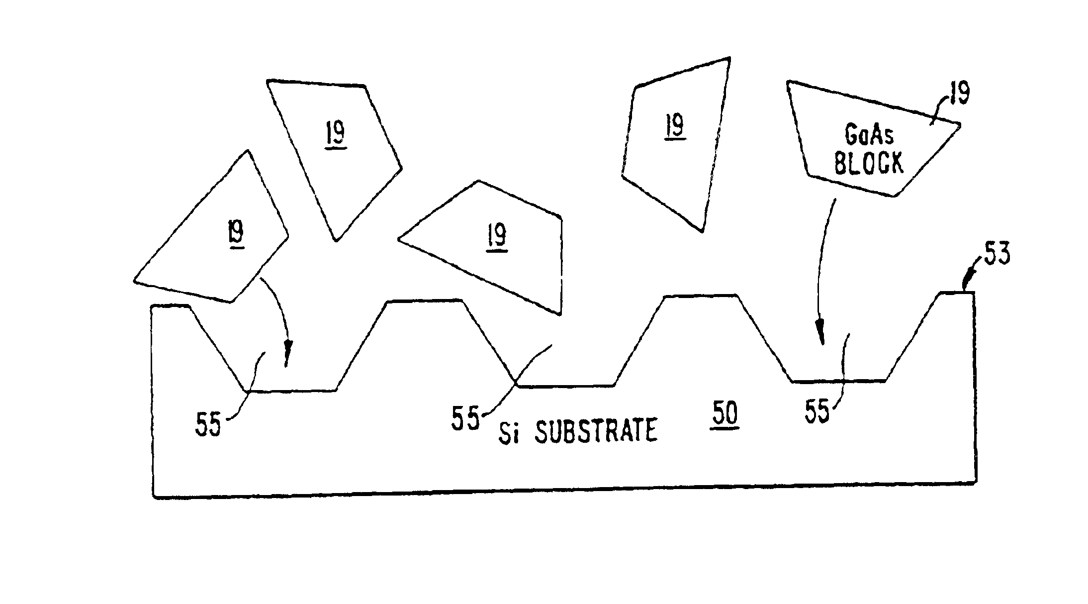
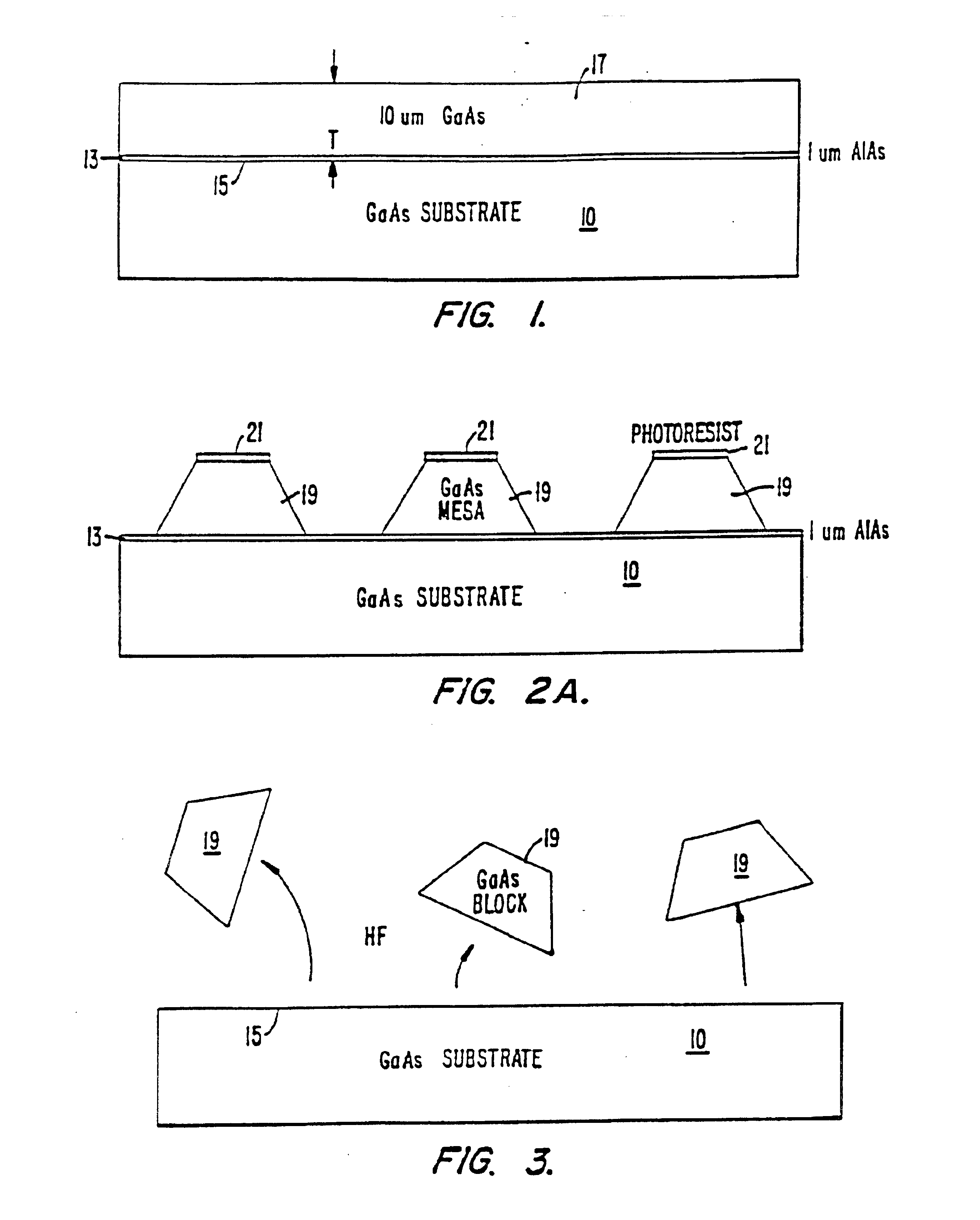
To prove the principle and demonstrate the operation of the method and structure, a gallium arsenide block in the form of a diode was assembled onto a silicon substrate and operated.

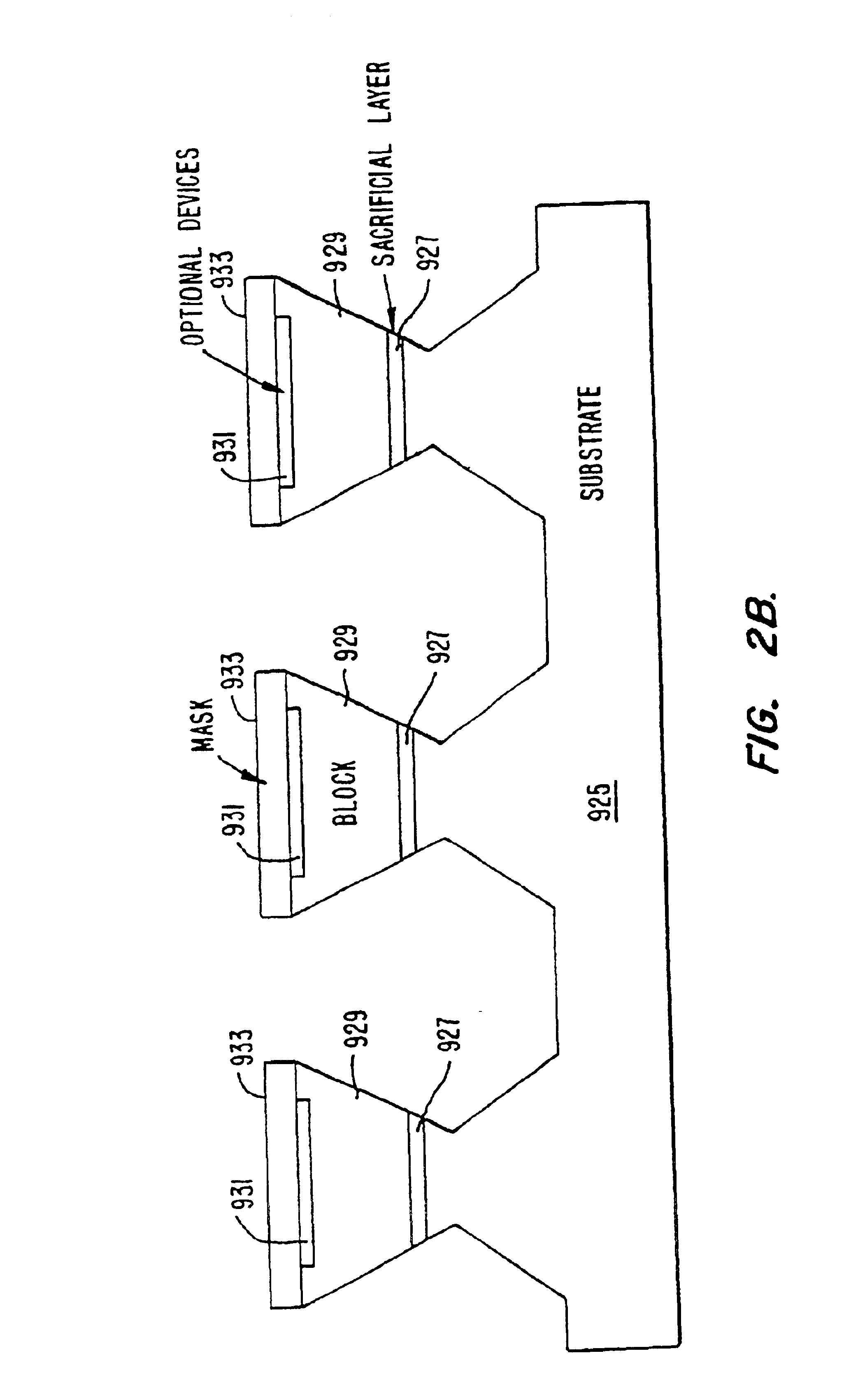
In a gallium arsenide example, a slurry including gallium arsenide blocks were transferred such that the blocks self-aligned into recessed regions located on a top surface of a silicon substrate. The steps for such method included forming the gallium arsenide blocks, transferring the blocks into a solution forming a slurry, and transporting the slurry evenly over a top surface of a silicon substrate having recessed regions. The shaped blocks generally tumble onto the top surface of the substrate, self-align and engage with a recessed region having a complementary shape.

In creating the silicon substrate, a solution of ethylenediamine pyrocatechol pyrazine (EDP) or potassium hydroxide (KOH) produced recessed regions having a trapezoidal profile or inverted truncated pyramid shape. Each solution created tra...


PUM

PropertyMeasurementUnit
lengthaaaaaaaaaa
lengthaaaaaaaaaa
lengthaaaaaaaaaa

Abstract

A method and apparatus for assembling microstructures onto a substrate through fluid transport. The microstructures being shaped blocks self-align into recessed regions located on a substrate such that the microstructure becomes integral with the substrate. The improved method includes a step of transferring the shaped blocks into a fluid to create a slurry. Such slurry is then dispensed evenly or circulated over the top surface of a substrate having recessed regions thereon. The microstructure via the shape and fluid tumbles onto the surface of the substrate, self-aligns, and engages into a recessed region.

Description

BACKGROUND OF THE INVENTIONThe present invention relates to the field of electronic integrated circuits. The invention is illustrated in an example with regard to the manufacture of gallium arsenide microstructures onto a silicon substrate, but it will be recognized that the invention will have a wider range of applicability. Merely by way of example, the invention may be applied in the manufacture of devices containing silicon based electronic devices integrated with a gallium arsenide based microstructures (or devices) such as light emitting diodes (LED), lasers, tunneling transistors, Gunn oscillators, integrated circuits, solar collectors, liquid crystal displays (LCDs), and others.Industry currently needs a cost effective, efficient, and practical method for assembling a higher cost microstructure onto a lower cost commercially available substrate. In particular, a material such as gallium arsenide possesses substantially better characteristics for some specific electronic and ...

Claims


Application Information

Patent Timeline
Patent Type & Authority Patents(United States)
IPC IPC(8): G02F1/13G02F1/1362H01L21/70H01L25/065H01L21/68H01L23/13H01L21/02H01L23/14H01L21/67H01L21/58H01L23/12H01L21/98G02F1/136G02F1/1368H01S5/40H01S5/00H01S5/022H01L29/06
CPCG02F1/1362H01L21/02002H01L21/6835H01L23/13H01L23/147H01L24/24H01L24/26H01L24/82H01L24/83H01L24/95H01L25/0655H01L25/50G02F1/136H01L2924/10253Y10S438/978H01L2924/12041H01L2924/014H01L2924/01072H01L2924/01033H01L2924/01023G02F1/1368H01L29/0657H01L2221/68359H01L2224/24227H01L2224/83136H01L2224/8319H01L2224/8385H01L2224/95085H01L2224/95092H01L2224/95122H01L2224/95136H01L2924/01005H01L2924/01013H01L2924/01015H01L2924/01018H01L2924/0102H01L2924/01027H01L2924/01032H01L2924/01047H01L2924/01049H01L2924/01079H01L2924/01082H01L2924/01322H01L2924/07802H01L2924/09701H01L2924/10158H01L2924/10329H01L2924/14H01L2924/15153H01L2924/15155H01L2924/15157H01L2924/15165H01L2924/30105H01L2924/30107H01L2924/01006H01L2924/01019H01L2924/3512H01L2924/00H01L2924/15787H01L2924/15788H01L2924/12042
Inventor SMITH, JOHN STEPHEN
Owner RGT UNIV OF CALIFORNIA
Why Eureka
Try Eureka