
Semiconductor device and method of manufacturing thereof

a semiconductor and capacitor technology, applied in the direction of coatings, transistors, chemical vapor deposition coatings, etc., can solve the problems of inability to apply to the device process, lack of reproducibility, and the proper properties of these mim and mis capacitors

Inactive Publication Date: 2005-03-15
HITACHI LTD
View PDF11 Cites 13 Cited by
  • Summary
  • Abstract
  • Description
  • Claims
  • Application Information

AI Technical Summary

Benefits of technology

An object of the present invention is to provide a semiconductor device containing MIS or MIM capacitor having hexagonal phase and permittivity of 50 or more. More concretely, by using a dielectric film made of a solid solution of tantalum pentoxide and niobium pentoxide with a film thickness of 10 nm or less, the above object is attained.

Problems solved by technology

However, the high dielectric Ta2O5's mentioned above have problems mentioned below, respectively.
In addition, properties of these MIM and MIS capacitors are largely dependent on preparation conditions and heat treating conditions, and lack in reproducibility.
As to the addition of TiO2 and Al2O3, since high temperature heat treatment of 1400° C. is necessary, application to the device processes is impossible.

Method used


Image

  • Semiconductor device and method of manufacturing thereof
  • Semiconductor device and method of manufacturing thereof
  • Semiconductor device and method of manufacturing thereof

Examples


example 1

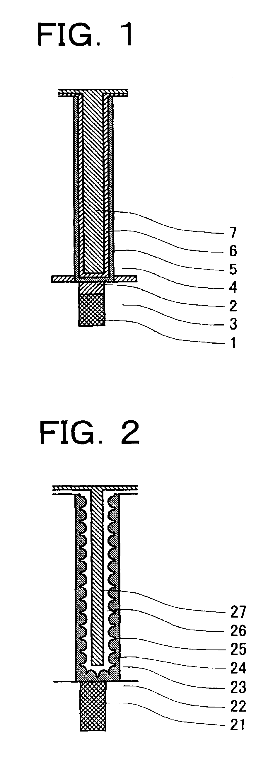
Example 1 is explained referring to FIG. 1. This Example is to explain steps for preparing capacitor using Pt or Ru electrode as a lower electrode and using a (Ta,Nb)2O5 solid-solution dielectric film with permittivity of as high as 50 or more as MIM capacitor. The solid-solution dielectric film was prepared by CVD method. The composition of solid solution was changed by independently transferring pentaethoxytantalum and pentaethoxyniobium. The explanation for steps before the formation of buried plug are omitted, since these steps are conventional.

On plug 1 to be laminated, Al-doped TiN barrier metal 2, and a plug portion interlaminar insulating layer 3 made of SiO2, a capacitor portion interlaminar insulating film 4 was deposited by plasma CVD method using a monosilane gas as a raw material. After forming a W film by sputtering, a resist was coated to process a W mask by a conventional photolithography, followed by dry etching of the capacitor portion interlaminar insulating film ...

example 2

Example 2 is explained referring to FIG. 2. This Example is to explain steps for preparing a capacitor using Ta2O5 or Nb2O5 dielectric film in a MIS capacitor using a polysilicon electrode covered with a silicon nitride film.

First, on a polysilicon plug 21 and a plug portion insulating layer 22 made of SiO2, a capacitor portion insulating film 23 made of SiO2 and having a film thickness of 2000 nm was deposited by plasma CVD method using monosilane gas as a raw material. After forming a W film by sputtering, a resist was coated to process a W mask by a conventional photolithography, followed by dry etching of the capacitor portion insulating film 23 until the surface of the polysilicon plug to form a deep concave for forming lower electrodes 24.

Next, an electroconductive amorphous silicon layer with a thickness of 20 nm was formed on inner surface of the deep concave and upper surface of the capacitor insulating film 23, followed by removal of the amorphous silicon layer on the uppe...

example 3

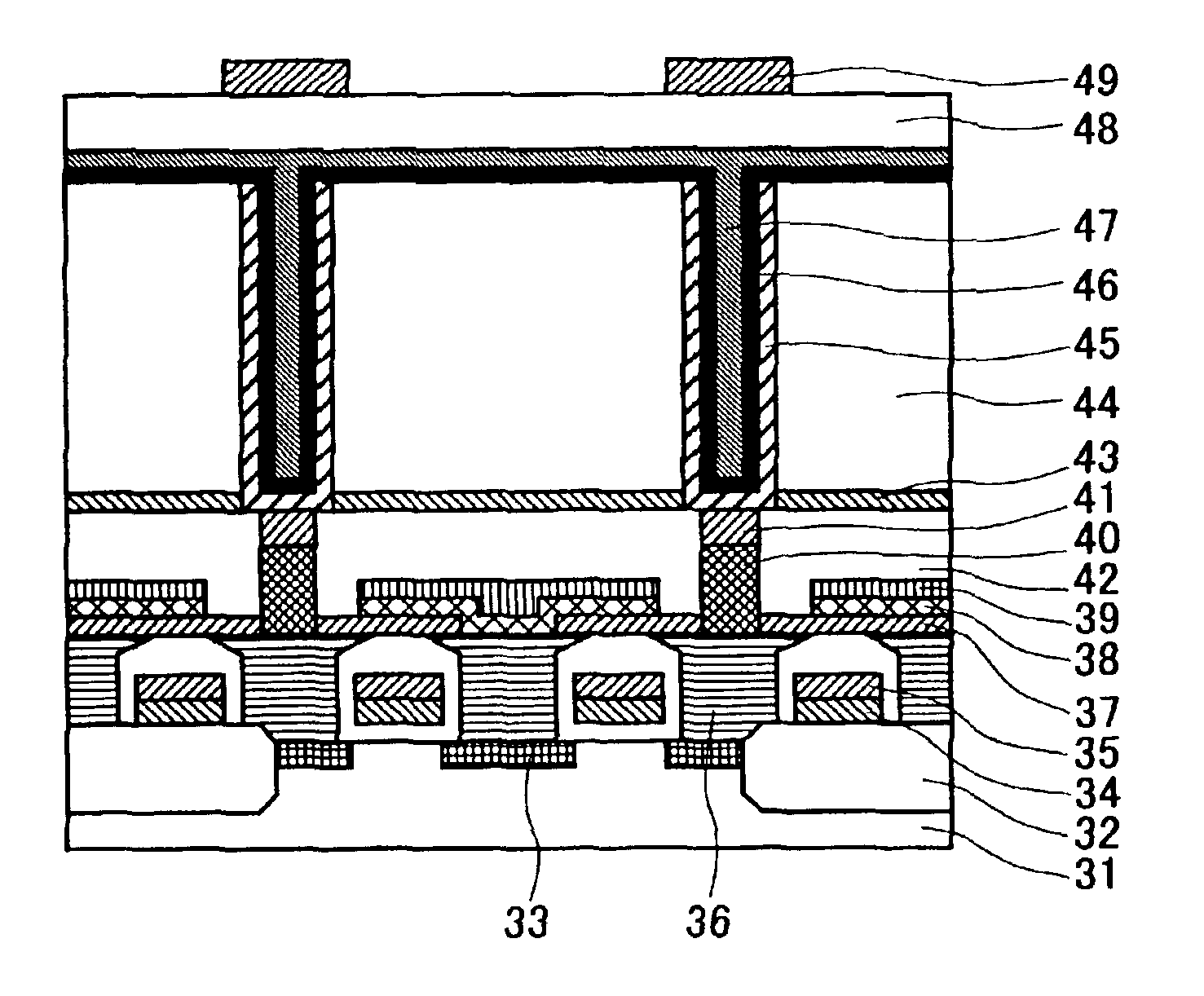
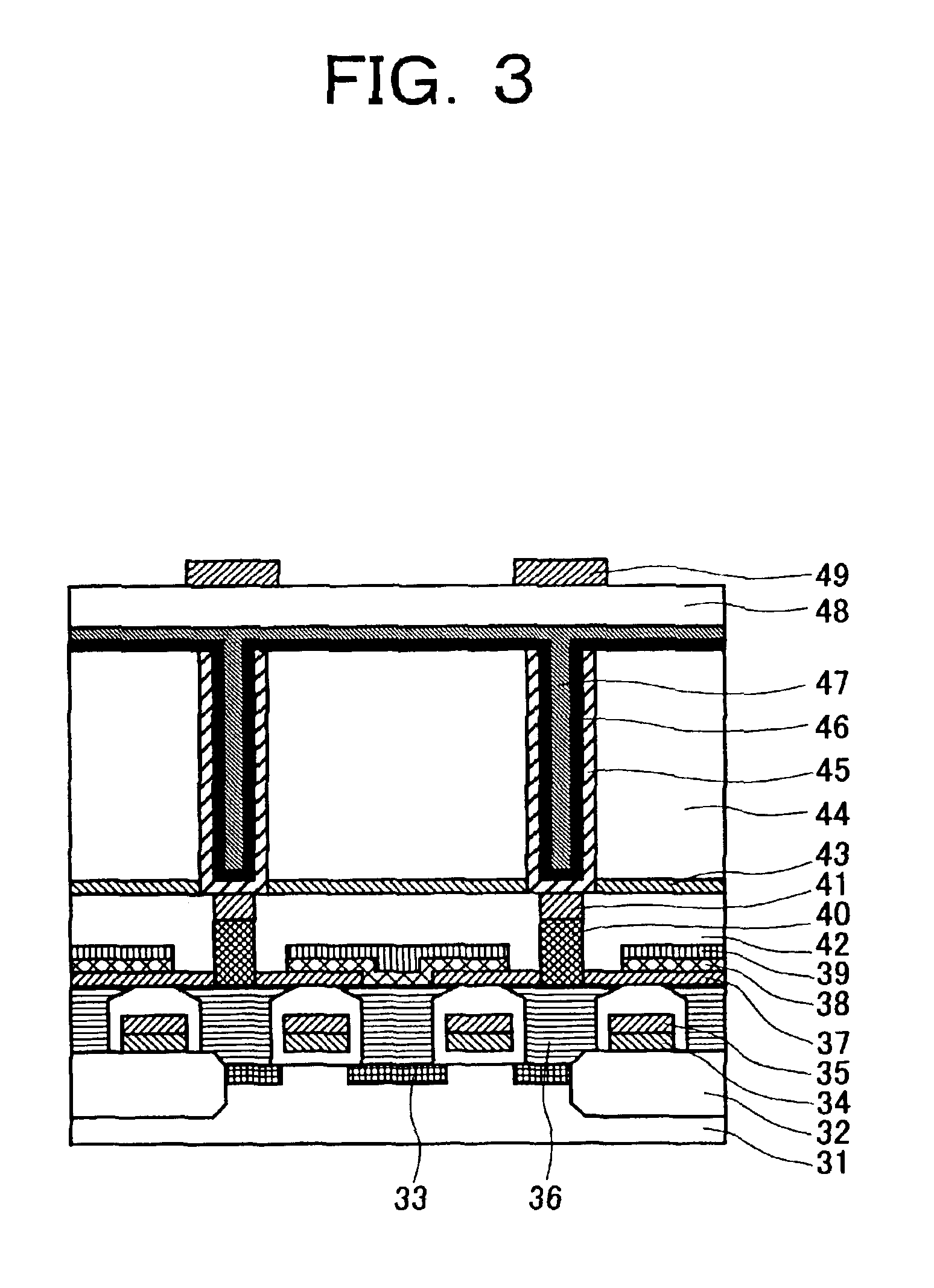
Example 3 is explained referring to FIG. 3. This Example is to explain a process for producing a semiconductor memory device containing MIM capacitor using a (Ta,Nb)2O5 solid-solution dielectric layer as capacitor insulating film. In the formation of a (Ta,Nb)2O5 solid-solution dielectric film by CVD method, this Example is characterized by using a cocktail of raw materials of pentaethoxytantalum and pentaethoxyniobium fed as a single raw material to give the solid-solution film with a predetermined composition.

On a silicon substrate 31, an isolation (SiO2) 32 by thermal oxidation and a diffusion layer 33 by ion doping were formed, followed by formation of a laminate of word line (polysilicon) 34 and word line (WSi2) 35 thereon. Then, on a barrier layer (Si3N4) 37, a bit line (polysilicon) 38 and a bit line (WSi2) 39 were formed. Further, in a plug portion insulating film 42 made of SiO2, a first plug (polysilicon) 36, a second plug (polysilicon) 40 and a barrier metal (TaN) 41 were...


PUM

PropertyMeasurementUnit
thicknessaaaaaaaaaa
temperatureaaaaaaaaaa

Abstract

By using a solid solution of tantalum pentoxide and niobium pentoxide as a dielectric film installed between upper electrode and lower electrode in a capacitor which is used in a semiconductor device, the capacitor structure can be simplified to improve reliability of the semiconductor device while reducing the production cost thereof.

Description

BACKGROUND OF THE INVENTIONThis invention relates to a semiconductor device containing a capacitor wherein a metal oxide of tantalum pentoxide, and the like, is used as dielectrics and a method for manufacturing thereof.In semiconductor devices having LSI such as dynamic random access memory (DRAM), etc., the capacitor area is reduced with higher integration. Thus, there is studied application of metal oxide dielectrics such as tantalum pentoxide (Ta2O5) having high permittivity of several tens in place of the silicon oxide which has been used as capacitor dielectric film. Further, in gigabit generation semiconductor devices wherein the minimum processing size is 0.15 μm or less, it is necessary to form a dielectric film by using a CVD (chemical vapor deposition) method on a surface of deep hole or concave in order to enhance capacitance, even if metal oxide dielectrics having a higher permittivity are used.High dielectric Ta2O5's applied so far can be summarized as follows.1) In a ...

Claims


Application Information

Patent Timeline
Patent Type & Authority Patents(United States)
IPC IPC(8): H01L21/02H01L21/316H01L27/108C23C16/40H01L21/8242
CPCH01L21/31604H01L21/31691H01L28/40H01L27/10814H01L21/02183H01L21/02192H01L21/02194H01L21/02271H10B12/315H10B12/00
Inventor HIRATANI, MASAHIKOKIMURA, SHINICHIROHAMADA, TOMOYUKI
Owner HITACHI LTD
Learn More