Organic electroluminescence device and manufacturing method therefor

a technology of electroluminescence device and manufacturing method, which is applied in the direction of discharge tube/lamp details, discharge tube luminescnet screen, organic semiconductor device, etc., can solve the problems of long life and low consumption of electric power, and achieve the effect of preventing the decrease of contrast, long life and low electric power

Inactive Publication Date: 2005-03-22
ELEMENT CAPITAL COMMERCIAL CO PTE LTD
View PDF26 Cites 147 Cited by
  • Summary
  • Abstract
  • Description
  • Claims
  • Application Information

AI Technical Summary

Benefits of technology

The invention solves the problems described above, and an object of the present invention is to provide an arrangement of elements in which the aperture ratio and the light transmittance are not degraded even when a switching element is used. It is also an object of the invention to provide a manufacturing method thereof. In other words, an organic EL device is provided which consumes low electric power and has a long life. In addition, a structure is also proposed in which a decrease in contrast is prevented, which is caused by incident outside light, without decreasing the luminance.

Problems solved by technology

In other words, an organic EL device is provided which consumes low electric power and has a long life.

Method used


Image

  • Organic electroluminescence device and manufacturing method therefor
  • Organic electroluminescence device and manufacturing method therefor
  • Organic electroluminescence device and manufacturing method therefor

Examples


embodiment 1

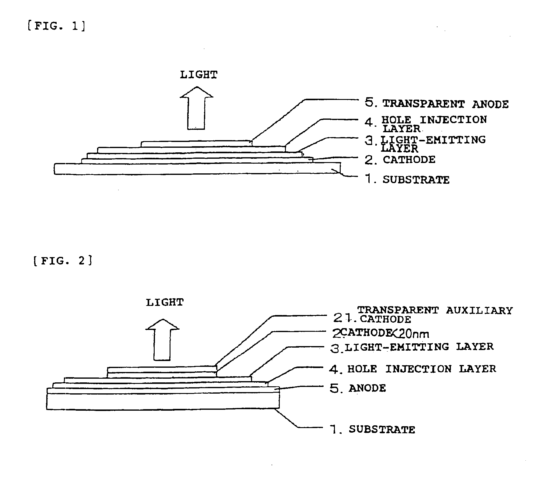
In this embodiment, an example will be described in which at least a cathode, a light-emitting layer, a transparent anode, and a hole transport layer and / or a hole injection layer are formed on a substrate in this order. In FIG. 1, a cross-sectional view of an organic EL device according to this embodiment is shown.

First, a cathode 2 was formed on a substrate 1. Next, a light-emitting layer 3 was formed, and in addition, a hole injection layer 4 was formed. Next, an anode 5 was formed, and in addition, a sealing layer (not shown in the figure) was formed.

When a voltage was applied between electrodes of the organic EL device thus formed, light was emitted from the sealing layer side.

For the substrate 1 used in this embodiment, in addition to a glass substrate, a metal, a semiconductor, a plastic, or the like may be used, and an opaque substrate may also be used.

For the cathode 2 used in this embodiment, aluminum, magnesium, lithium, or calcium may be used, and in addition, the alloy ...

embodiment 2

In this embodiment, a particular example will be described in which the cathode is formed of a laminate formed of at least one type of conductive material and a metal oxide or fluoride. By using the method of Embodiment 1, when patterning was performed in a photolithographic step after an aluminum film was formed as a cathode, and an oxygen plasma treatment was then performed, an oxide layer 20 Å thick was formed on the surface. By using this substrate provided with the cathode, when an organic EL device was formed by performing the outstanding steps in Embodiment 1, the luminous efficiency thereof was two times (0.2 lm / W) that obtained in Embodiment 1.

Instead of the oxygen plasma treatment performed on the surface of the cathode, when lithium fluoride 20 Å thick was deposited, the luminous efficiency was 0.5 lm / W.

The light-emitting layer 3 used in this embodiment was formed of a polyfluorene material and was formed by spin coating. The hole injection layer 4 was formed by spin coat...

embodiment 3

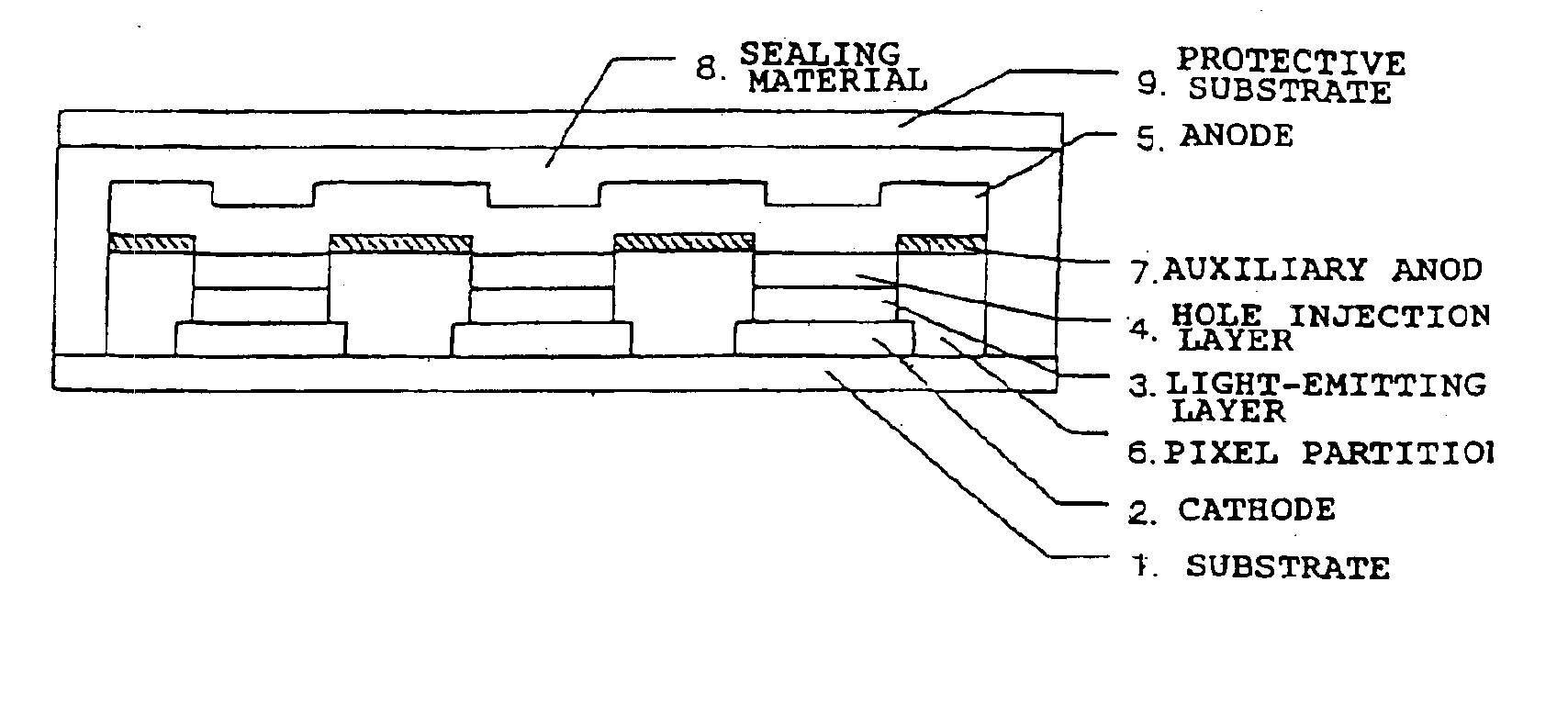
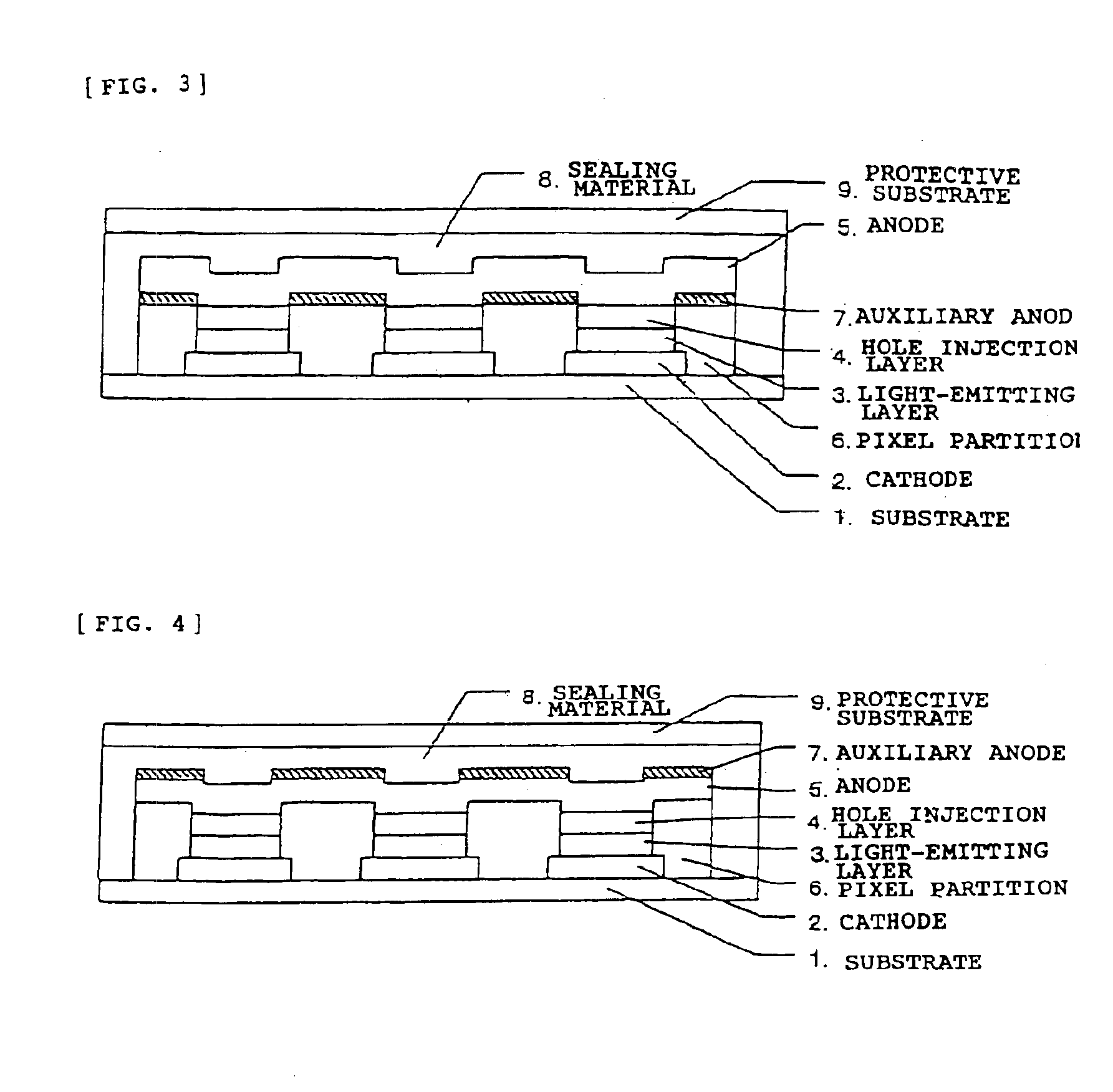
In this embodiment, an example of the structure shown in FIG. 3 will be described in which a plurality of cathodes 2 corresponding to a plurality of light-emitting pixels are formed on a substrate 1, pixel partitions 6 formed of an insulating material are formed between the light-emitting pixels, and auxiliary anodes 7 formed of a conductive material having approximately equivalent patterns to those of the pixel partitions 6 are formed thereon.

A particular example is described below. First, after the cathodes 2 were patterned, the pixel partitions 6 were formed of a polyimide and were patterned, and subsequently, a film formed of tantalum 1,000 Å thick was formed and was then patterned so as to form the same pattern as that of the pixel partition 6. Next, a film formed of lithium fluoride 20 Å thick was formed on the entire surface, three types of polyfluorene materials emitting red, green, and blue light were each dissolved in isodurene, and the films thereof as the light-emitting ...


PUM


Abstract

An organic EL device in accordance with the invention has a structure in which a first electrode, a light-emitting layer, and a second electrode are formed on a substrate in this order, and light from the light-emitting layer is emitted to an exterior of the device via the second electrode.

Description

BACKGROUND OF THE INVENTION1. Field of the InventionThe present invention relates to the structure of an electroluminescent (in this specification, referred to as organic EL) device for use as a display device in an information terminal apparatus, such as a computer, a mobile phone, or a television, and also relates to a manufacturing method thereof.2. Background of the Related ArtRecently, there has been an increasing trend toward portability of information terminals, and development of power saving displays, which are necessary to enhance portability. Among displays, organic EL displays in particular have drawn attention, and the development thereof is at the stage of pursuing practical applications.In order to realize power saving displays, it is believed that it is most effective to drive an organic EL element by an active element, such as a thin-film transistor (TFT). The reason for this is that, when an active element is used, an organic EL element can be driven by a DC voltag...

Claims


Application Information

Patent Timeline
Patent Type & Authority Patents(United States)
IPC IPC(8): H01L51/52H01L51/50H05B33/14H01L27/32H01L27/28
CPCH01L51/5206H05B33/14H01L27/3244H01L27/3281H01L51/5284H01L2251/5315H01L51/5237H10K59/12H10K59/17H10K50/814H10K50/841H10K50/865H10K2102/321H10K2102/3026H01L31/12H05B33/26
Inventor KOBAYASHI, HIDEKAZU
Owner ELEMENT CAPITAL COMMERCIAL CO PTE LTD
Why Eureka
Try Eureka