

Electromagnetic wave absorber
- Summary
- Abstract
- Description
- Claims
- Application Information
AI Technical Summary
Benefits of technology
Problems solved by technology
Method used
Image

Examples
example
Examples of the invention are given below by way of illustration and not by way of limitation. EM is an abbreviation of electromagnetic wave.
examples 1-5
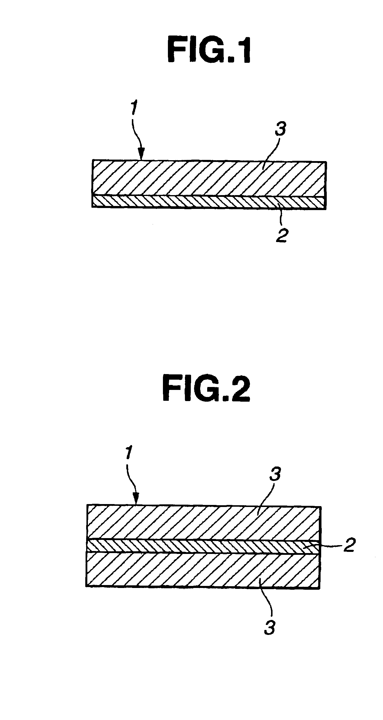
An EM absorber of the two layer structure was fabricated as follows which included an EM-reflecting layer formed of a silicone resin having an electrically conductive filler and a heat conductive filler dispersed therein and an EM-absorbing layer formed of a silicone resin having an EM-absorbing filler and a heat conductive filler dispersed therein.
A liquid composition of the addition reaction type was prepared using 100 parts by weight of a vinyl-containing dimethylpolysiloxane blocked at either end with a dimethyl vinylsiloxy radical and having a viscosity of 30 Pa·s at room temperature as the base oil. An organopolysiloxane containing silicon atom-bonded alkoxy radicals as the surface treating agent for an electrically conductive filler and a heat conductive filler was added to the base oil in an amount of 1 part per 100 parts by weight of the electrically conductive filler and heat conductive filler combined. Then the electrically conductive filler and heat conductive filler wer...
examples 6-10
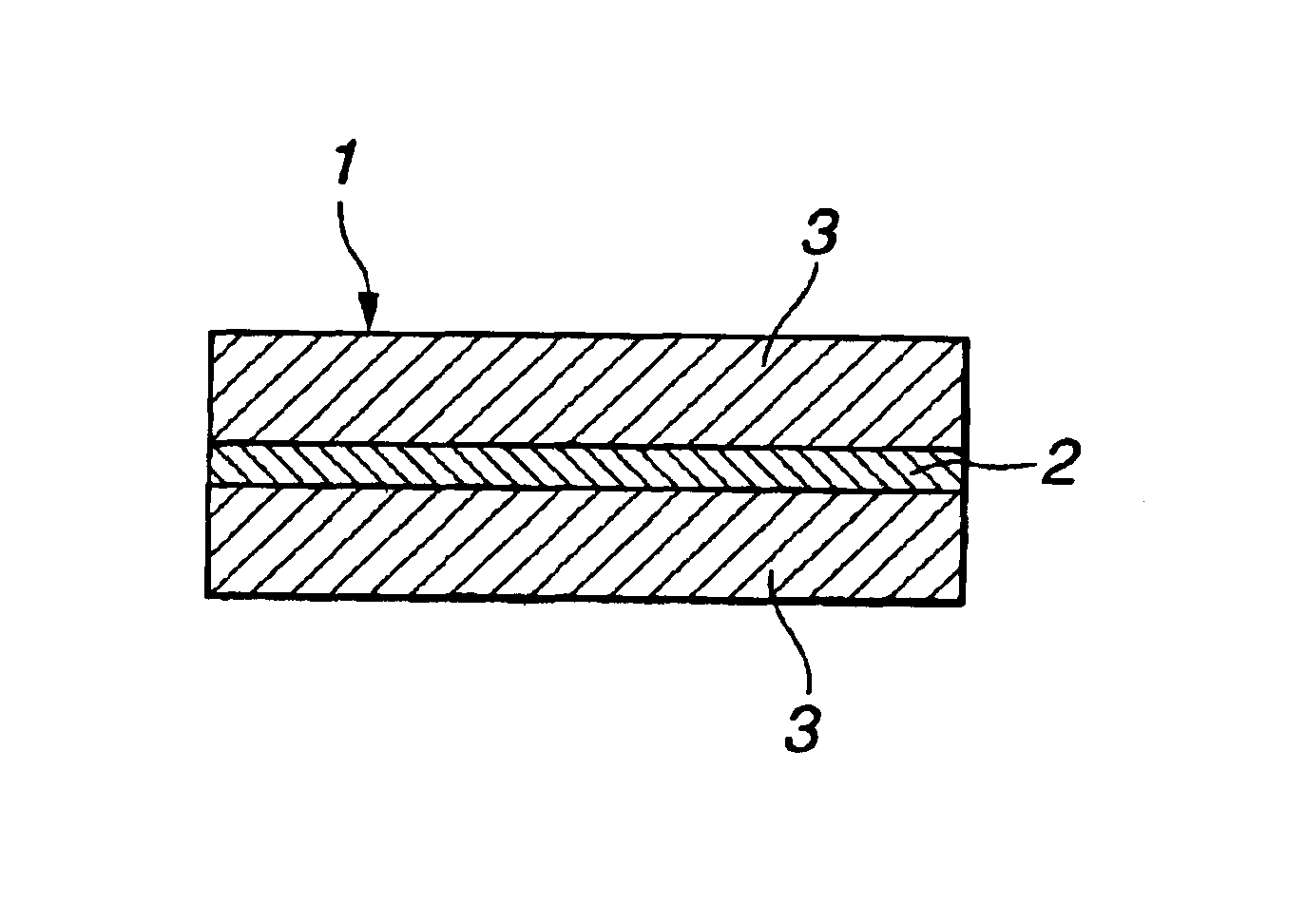
An EM absorber of the integrated three-layer structure consisting of the EM-absorbing layers on either surface of the EM-reflecting layer as shown in FIG. 2 was obtained by following the procedure of Examples 1-5 except that the EM-absorbing layer was formed on each surface of the EM-reflecting layer.
The composition and thickness of the EM-absorbing layer and the EM-reflecting layer are shown in Table 1.
PUM
| Property | Measurement | Unit |
|---|---|---|
| Percent by volume | aaaaa | aaaaa |
| Percent by volume | aaaaa | aaaaa |
| Particle size | aaaaa | aaaaa |
Abstract
Description
Claims
Application Information