Method for forming capacitor

a capacitor and dielectric technology, applied in the field of capacitor formation, can solve the problems of providing a method for forming a capacitor with a high capacitance, and the use of capacitor dielectrics, and achieve the effect of large capacitance valu

Inactive Publication Date: 2005-04-05
RENESAS ELECTRONICS CORP
View PDF10 Cites 28 Cited by
  • Summary
  • Abstract
  • Description
  • Claims
  • Application Information

AI Technical Summary

Benefits of technology

[0026]The capacitors formed using the methods for forming a capacitor according to the first through third aspects of the invention each include one insulating film having dielectric constant not less than 25 and an alternative insulating film having dielectric constant not less than 50. In this case, the flow of electrons within the one insulating film occurs by the so-called Fowler-Nordheim (F-N) tunnelling mechanism or by a direct tunneling mechanism and is affected to a small extent by variations in ambient temperatures, and the flow of electrons within the alternative insulating film is affected to a large extent by variations in ambient temperatures. Accordingly, those insulating films form a capacitor having a large

Problems solved by technology

However, the capacitor dielectrics employed in the first and second conventional examples cannot satisfy the requirements that a DRAM capacitor has a high capacitance and at the same time, allows leakage current flowing there though to be maintained at a low level.
More

Method used


Image

  • Method for forming capacitor
  • Method for forming capacitor
  • Method for forming capacitor

Examples


second embodiment

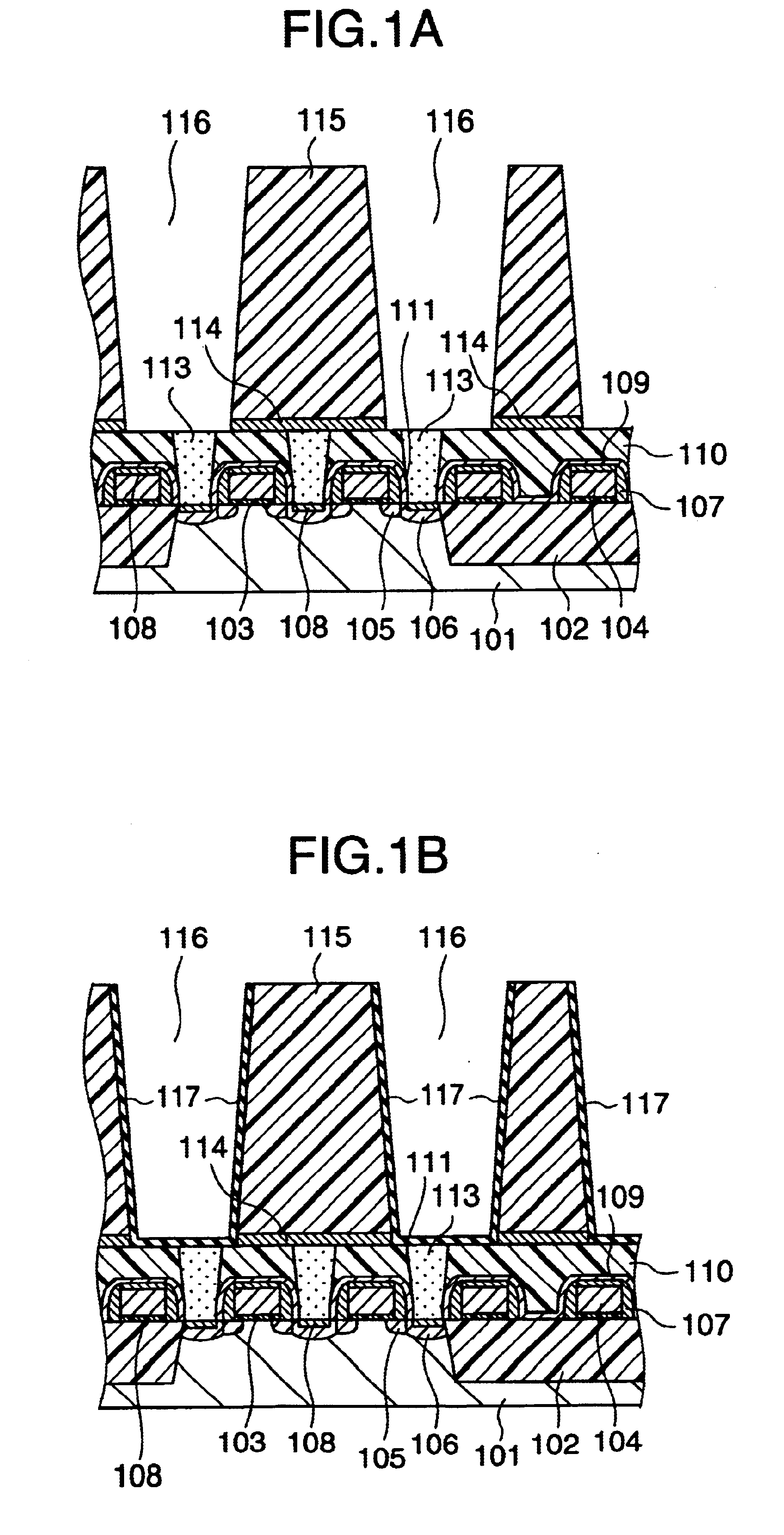
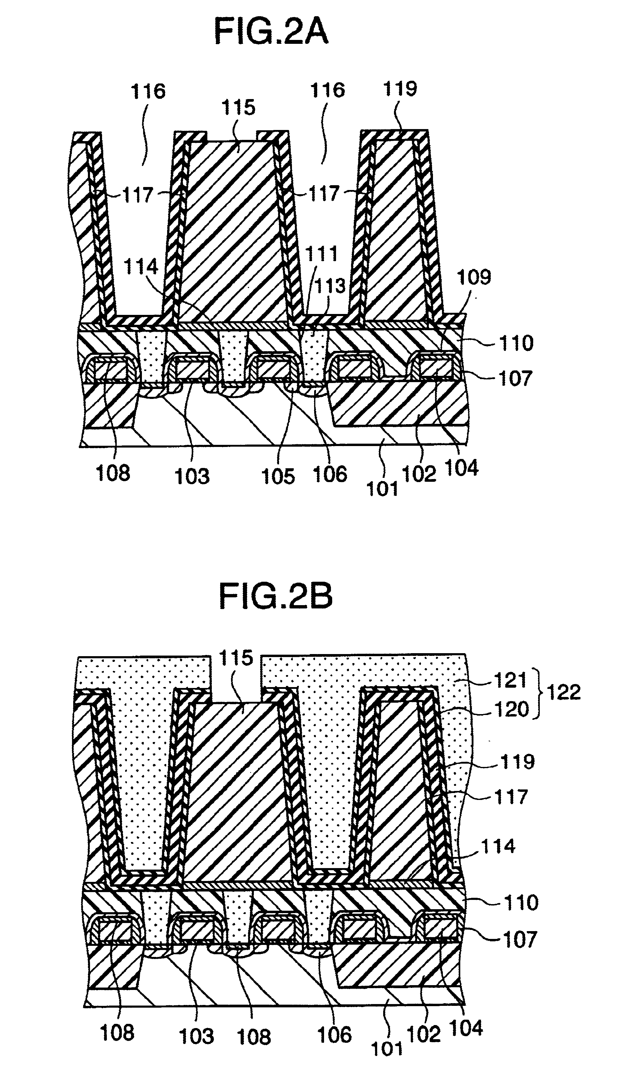
[0041]FIGS. 11A, 11B are cross sectional views of a capacitor formed using the method according to the invention in the order of manufacturing steps;

[0042]FIGS. 12A, 12B are cross sectional views illustrating the steps subsequent to the step of FIG. 11B;

third embodiment

[0043]FIGS. 13A, 13B are cross sectional views of a capacitor formed using the method according to the invention in the order of manufacturing steps;

[0044]FIGS. 14A-C are illustrations of how the capacitors formed using the methods, related to formation of capacitor, according to the first through third embodiments allow leakage current to flow therethrough; and

[0045]FIG. 15 illustrates how capacitance per unit area varies depending on the capacitor formation methods employed in the first and second conventional examples and the first through third embodiments.

DETAILED DESCRIPTION OF THE PREFERRED EMBODIMENTS

first embodiment

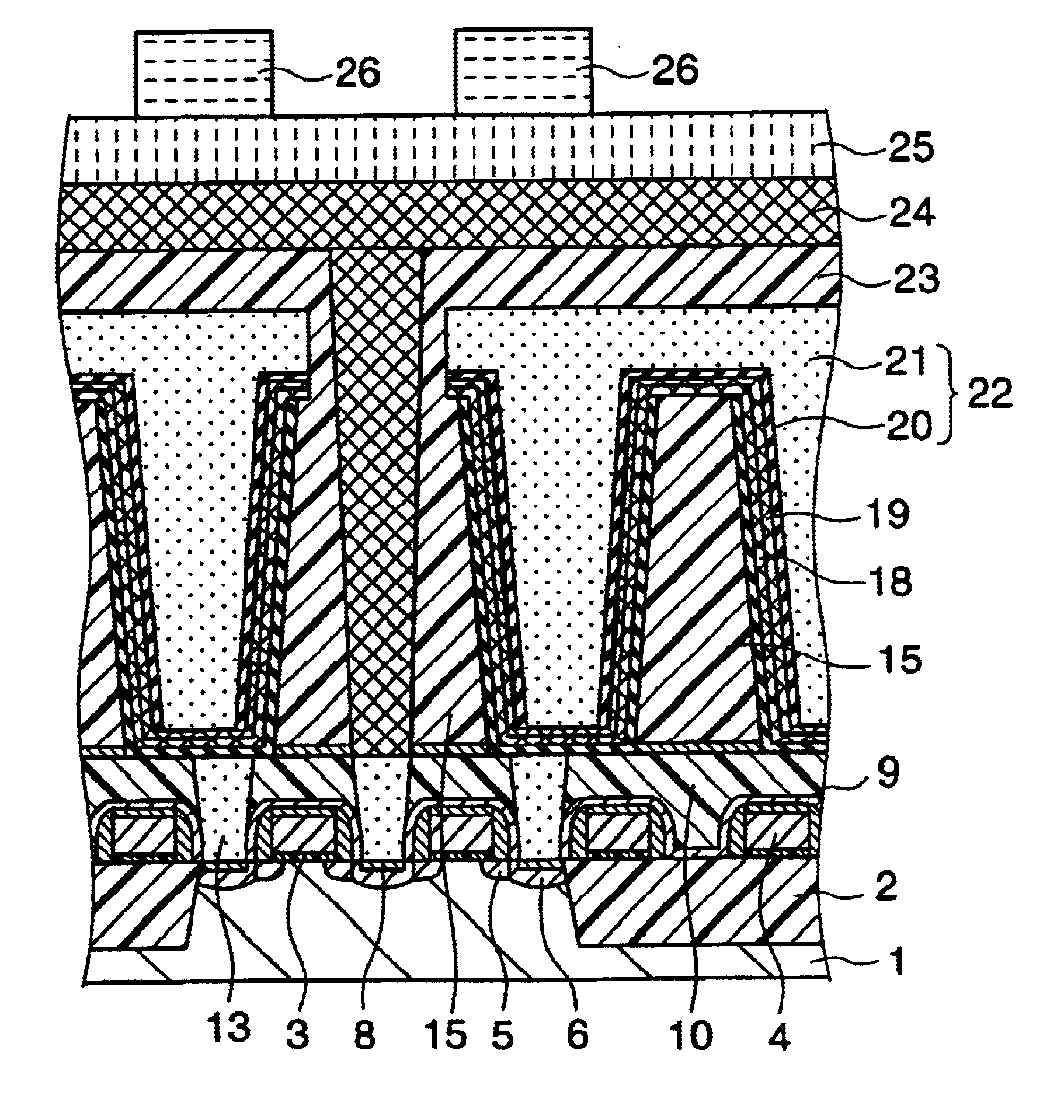
[0046]A method for forming a capacitor according to the invention will be explained with reference to FIGS. 5 through 10 illustrating cross sectional views of associated manufacturing steps.

[0047]First, in accordance with a process known to those skilled in the art, gate oxide films 3 and gate electrodes 4 are formed on a region that is separated from other regions by a field isolation film 2 in a silicon substrate 1 (FIG. 5A).

[0048]Subsequently, LDD regions 5 and diffusion layers 6 are formed in regions of the silicon substrate 1 on both sides of the gate electrode 4 to create a MOSFET. Furthermore, cobalt salicide layers 8 are formed in surface portions of the gate electrodes 4 and the diffusion layers 6 using typical Self Aligned Silicide (Salicide) techniques (FIG. 5C). The above-stated cobalt salicide layers are formed according to the following process steps.

[0049]An insulating film 7 made of, for example, SiO.sub.2 is deposited using CVD techniques, etc. to cover upper surfac...


PUM


Abstract

A capacitor is provided that is optimal for use in DRAM and has high dielectric constant, and allows leakage current flowing therethrough to be maintained at a low level, and further, permits dependence of the leakage current on temperatures to be small. That is, capacitor openings are formed in an inter layer silicon oxide layer and a TiN film is patterned so that TiN films are left only within the openings to form lower electrodes within the openings. Subsequently, a Zr- and/or Hf-containing oxide film (represented by the formula, multicomponent Zr.sub.x.Hf.sub.1-x.O.sub.2 film (0≦x≦1)) formed from a metal-containing organic compound as a reactant and a Ti-containing oxide film are laminated to form capacitor dielectrics. After deposition of the Zr- and/or Hf-containing oxide film, the Zr- and/or Hf-containing oxide film is subjected to heat treatment to be performed in an oxidizing ambient to remove residual carbon being retained in the Zr- and/or Hf-containing oxide film, leading to formation of a capacitor that is optimal for use in DRAM and has high dielectric constant, and allows leakage current flowing therethrough to be maintained at a low level.

Description

BACKGROUND OF THE INVENTION[0002]1. Field of the Invention[0003]The present invention relates to a method for forming a capacitor, and particularly to a method for forming a capacitor having a Metal-Insulator-Metal (MIM) structure in which metal or metal nitride films are employed as upper and lower electrodes.[0004]2. Description of the Related Art[0005]As DRAM components are fabricated with higher density processes, capacitors are also formed to be smaller in size. Accordingly, a dielectric material, having dielectric constant greater than that of SiO.sub.2, such as Al.sub.2 O.sub.3, TiO.sub.2, (Ba, Sr)TiO.sub.3, Pb(Zr, Ti)O.sub.3, is employed as capacitor dielectrics. In addition to the capacitor dielectrics having a high dielectric constant, upper and lower electrodes made of noble metal to reduce leakage current are provided to form a capacitor having a high dielectric constant.[0006]First, explanation will be made of an example (referred to as a first conventional example) of ...

Claims


Application Information

Patent Timeline
IPC IPC(8): H01L21/20H01L21/70H01L21/02H01L21/8242H01L27/108H01L21/316
CPCH01L27/10811H01L28/91H01L27/10852H01L27/10885H10B12/312H10B12/033H10B12/482
Inventor IIZUKA, TOSHIHIROYAMAMOTO, TOMOE
Owner RENESAS ELECTRONICS CORP
Why Eureka
Try Eureka