Microwave switching with illuminated field effect transistors

a field effect transistor and microwave switching technology, applied in the direction of multiple-port active networks, transmitter/receiver shaping networks, transmission, etc., can solve the problems of slow on/off charging of surface fault centers, requiring but little control power,

Active Publication Date: 2005-04-05
ROHDE & SCHWARZ GMBH & CO KG
View PDF3 Cites 22 Cited by
  • Summary
  • Abstract
  • Description
  • Claims
  • Application Information

AI Technical Summary

Benefits of technology

In accord with the invention, field effect transistors, which are integrated on a semiconductor chip, are subjected to light radiation from a light source. This action is within a housing, impenetrable to ...

Problems solved by technology

Beyond this, they require but little control power.
The cause is the slow ON/OFF c...

Method used


Image

  • Microwave switching with illuminated field effect transistors
  • Microwave switching with illuminated field effect transistors
  • Microwave switching with illuminated field effect transistors

Examples


Embodiment Construction

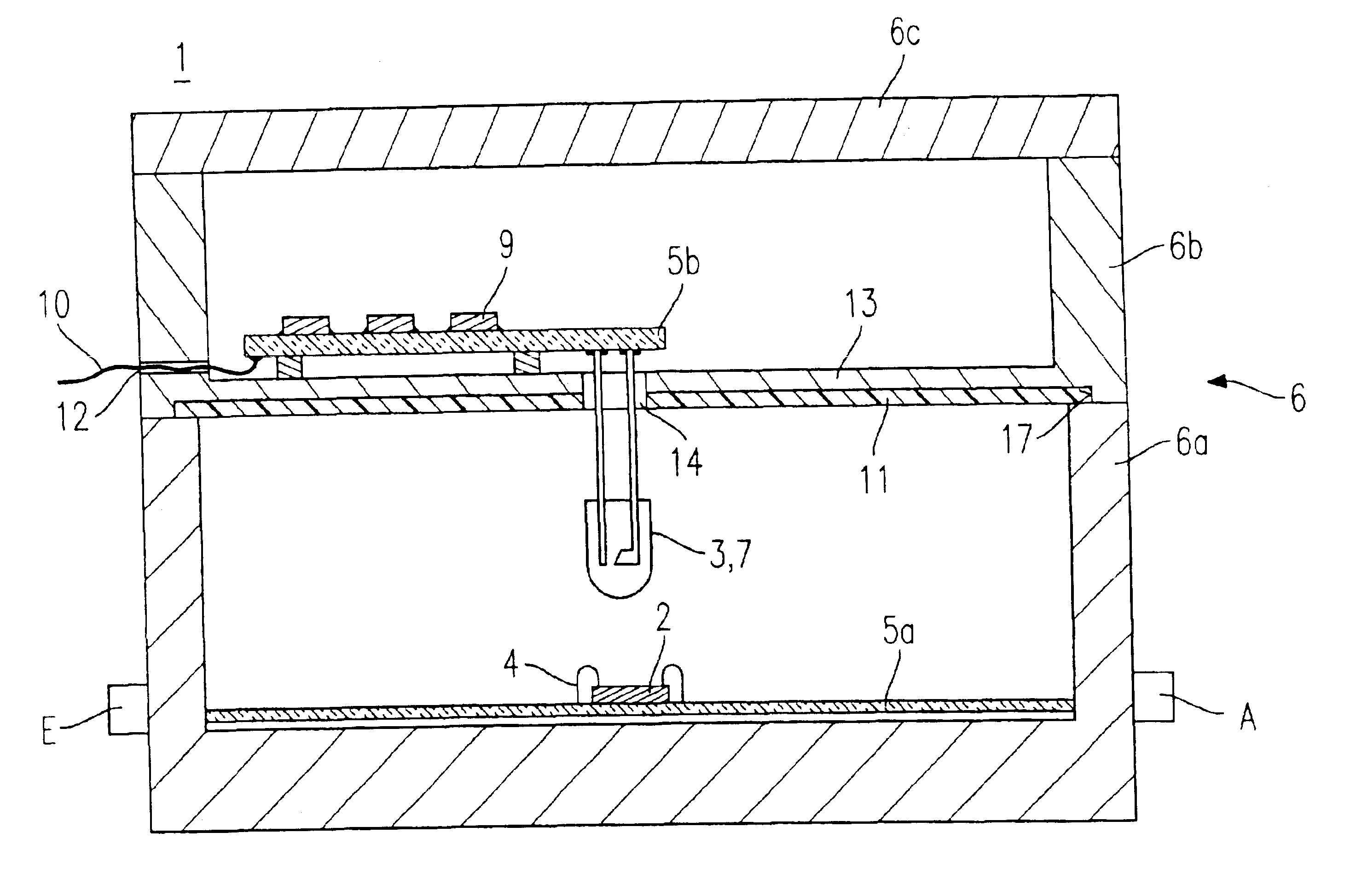
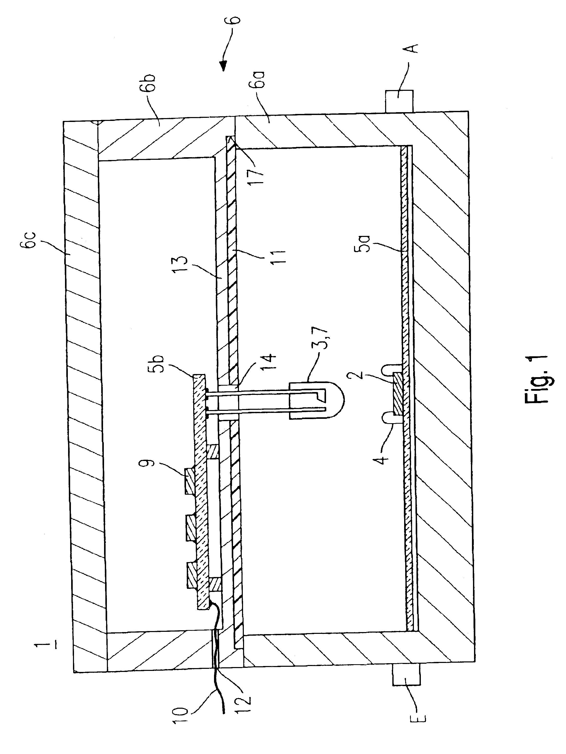
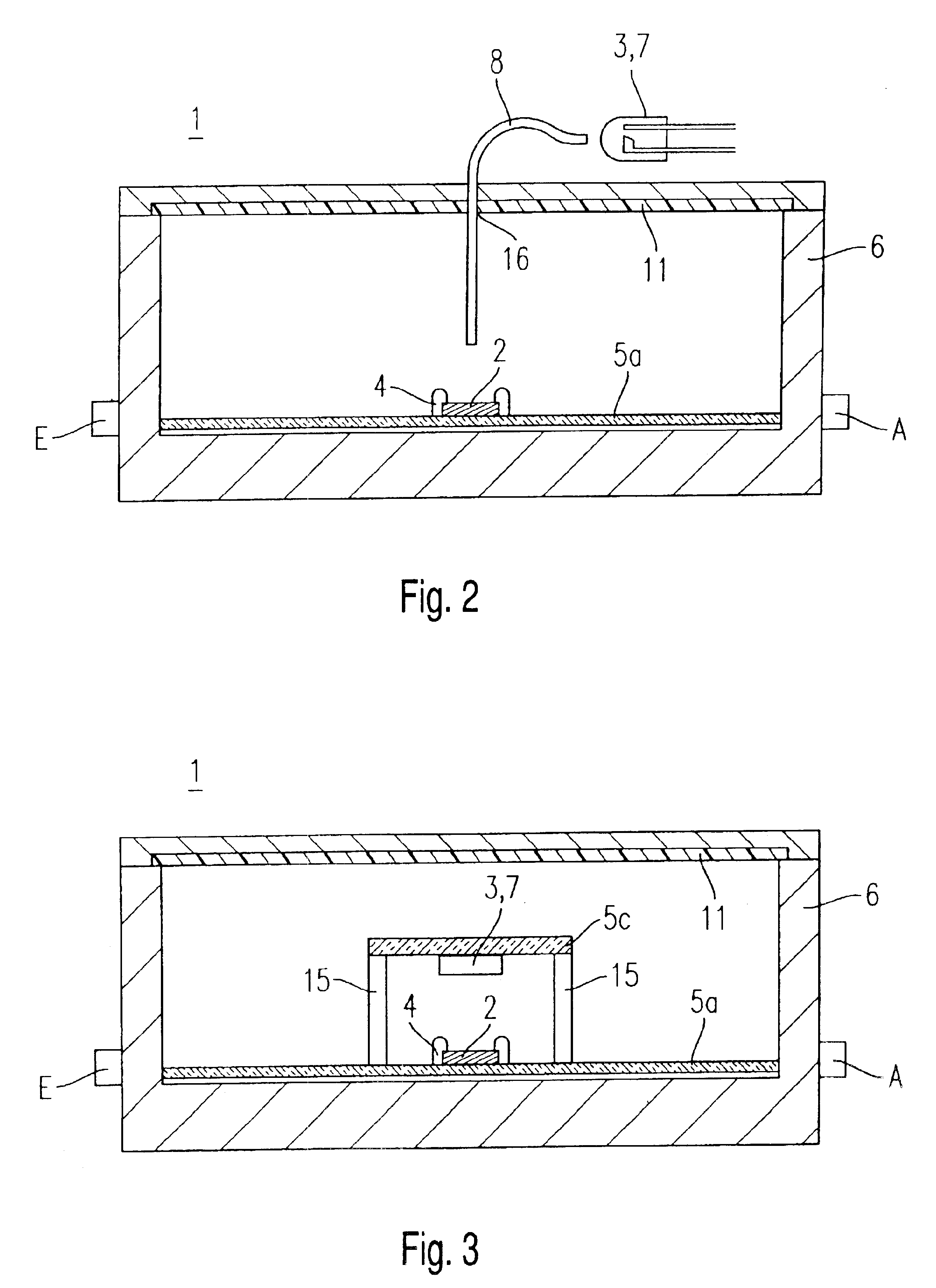
FIG. 1 shows an invented embodiment example of the electronic microwave circuit 1. A boxlike housing 6, depicted in sectional presentation, consists of a lower housing part 6a and an upper housing part 6b, wherein the bottom of lower housing part 6a holds a plate shaped substrate 5a. The semiconductor chip 2, which, for instance, possesses a damping circuit integrated thereupon, is mounted on the said substrate 5a. The said chip 2 is electrically connected by two contacting wires 4, which wires are in turn connected to (not shown) conductor paths running on the substrate 5a. Input E and output A which are connected to the circuit which is integrated on the semi conductor chip 2 are led to the outside through the lower housing piece 6a in microwave protected conductors.

The two boxlike housing pieces 6a, 6b are bound together with a cover piece 6c to exclude external, interfering microwaves. The interior chamber is separated by a bottom 13 of the upper housing piece 6b, wherein this s...


PUM


Abstract

An electronic microwave circuit (1) with field effect transistors which are integrated on at least one semiconductor chip (2), has a light source (3), which radiates the field effect transistors with light and possesses a housing (6) which encloses in a microwave excluding manner the semiconductor chip (2) and the light source (3) or a light conducting means (8) connected with the light source (3).

Description

BACKGROUND OF THE INVENTIONThe invention concerns a microwave circuit with field effect transistors, which circuit especially, but not exclusively, is designed as a damping circuit.Damping circuits are, for example, applied in high frequency technology for the purposes of measuring and control of levels in sending equipment and mobile radio apparatuses. In order, for example, to be able to quickly run through measurement sequences with different, changing parameters, the damping circuit, that is to say, the damping elements which are to be found therein, must be switched in very rapidly and possess a wide breadth of dynamics.For instance, such a damping element circuit has been made known by U.S. Pat. No. 5,157,323. The digitally controlled damping member disclosed therein is constructed with field effect transistors used as switching elements.This digital damping member of U.S. Pat. No. 5,157,323 is found disadvantageous on the basis of the relatively long switching time of the fie...

Claims


Application Information

Patent Timeline
IPC IPC(8): H03H11/24H03H11/04H03H11/14H03H11/02H03K17/16H03K17/687H01P1/10H03K17/041H03K17/04H01P1/15
CPCH01P1/15H03H11/245H03K17/6871H03K17/162H03K17/04106H01L2224/48091H01L2924/16195H01L2924/00014
Inventor EVERS, CHRISTIANCOHRS, WOLFGANGHECHTFISCHER, GERDHASSLER, MARTINWILL, THOMAS
Owner ROHDE & SCHWARZ GMBH & CO KG
Why Eureka
Try Eureka