Method and mold for manufacturing semiconductor device, semiconductor device and method for mounting the device

a manufacturing method and semiconductor technology, applied in semiconductor devices, semiconductor/solid-state device details, electrical apparatus, etc., can solve the problems of affecting difficult to handle and test protruding electrodes, and liable to scratches, so as to improve the reliability of electrical contacts, prevent flying leads from being deformed, and improve the effect of reliability

Inactive Publication Date: 2005-04-19
SOCIONEXT INC
View PDF156 Cites 88 Cited by
  • Summary
  • Abstract
  • Description
  • Claims
  • Application Information

AI Technical Summary

Benefits of technology

[0017]By the resin sealing step, the protruding electrodes which are too delicate to be subjected to a handling test are sealed by the resin layer. The resin layer realizes a surface protection and functions to relax stress generated at interfaces between the electrodes of the semiconductor element and the protruding electrodes. The subsequent protruding electrode exposing step exposes at least ends of the protruding electrodes from the resin layer. When the protruding electrode exposing step is completed, the protruding electrodes can electrically be connected to an external circuit board or the like. The subsequent separating step cuts the substrate on which the resin layer is formed together with the resin layer, so that the semiconductor elements are separated from each other. Hence, the individual semiconductor chips can be obtained. Since the resin layer is formed in the resin sealing step, it is not required to provide the under fill resin at the time of mounting the semiconductor device. Hence, the mounting operation can easily be carried out. The sealing resin used to form the resin layer is not provided in the narrow space between the semiconductor device and the mounting board, but is provided to the surface of the substrate on which the protruding electrodes are arranged and is thus shaped by molding. Hence, the resin layer can definitely be provided to the entire surface of the substrate on which the protruding electrodes are arranged. Since the resin layer functions to protect all the protruding, it is possible to definitely prevent connections between the protruding electrodes and the electrodes on the mounting board and connections between the protruding electrodes and the electrodes on the semiconductor element from being broken during a heating process. Thus, the reliability of the semiconductor device can be improved.
[0104]There is also provided a method for fabricating a semiconductor device, characterized by comprising: a semiconductor device main body forming step of forming a semiconductor device main body having a semiconductor element having a surface on which protruding electrodes are directly formed, and a resin layer which is formed on the surface of the semiconductor element and seals the protruding electrodes except for ends thereof; an interposer forming step of forming an interposer to which the semiconductor device main body is attached, a wiring pattern to which the semiconductor device main body is connected being formed on a base member of the interposer; a conductive member arranging step of arranging a conductive member to at least one of the semiconductor device main body and the interposer; a bonding step of bonding the semiconductor device main body and the interposer by an adhesive and connecting them electrically; and an external connection terminal forming step of forming external connection terminals which are connected to the wiring pattern through holes formed in the base member and are arranged on a surface of the semiconductor device main body opposite to the surface on which the protruding electrodes are provided. Since the resin layer is provided to the surface of the semiconductor device main body so that the ends thereof remain, the resin layer protects the semiconductor element and the protruding electrodes, and functions as an under fill resin. The semiconductor device main body is attached to the interposer, and the wiring pattern to which the semiconductor device main body is connected is formed on the base member. Hence, the wiring pattern can arbitrarily be formed on the base member. The external connection terminals are connected to the wiring pattern via the holes formed in the base member. Since the wiring pattern can arbitrarily be set, the external connection terminals can be determined independently of the positions of the protruding electrodes provided on the semiconductor device main body. Hence, the degree of freedom in layout of the external connection terminals can be increased. Further, the adhesive mechanically bonds the semiconductor device main body and the interposer, and the conductive member electrically bonds (connects) the semiconductor device main body and the interposer. As described above, the mechanical bonding and electrical bonding can separately be implemented by the respective members, so that substances respectively optimal to implementation of the functions (the mechanical bonding function and electrical bonding function) can be selected. Hence, the mechanical and electrical connections between the semiconductor device main body and the interposer can definitely be realized, and the reliability of the semiconductor device can be improved.

Problems solved by technology

The protruding electrodes 4 are formed of a soft metal such as solder, and are thus liable to take scratches.
Thus, it is difficult to handle and test the protruding electrodes.
Similarly, the semiconductor element 2 is in a bare chip formation and is thus liable to take scratches.
Thus, it is also difficult to handle and test the semiconductor element 2 as in the case of the protruding electrodes 4.
However, a troublesome filling work is required because the under fill resin 6 is provided in the narrow space 7 between the semiconductor element 2 and the mount board 5.
Further, it is difficult to uniformly provide the under fill resin 6 in the whole space 7.
Hence, the reliability in mounting is degraded.
A Further, the above semiconductor device 1 is mechanically weak and a low reliability because the semiconductor element 2 is mounted on the mount board 5 in a state in which the semiconductor element 2 is exposed.

Method used


Image

  • Method and mold for manufacturing semiconductor device, semiconductor device and method for mounting the device
  • Method and mold for manufacturing semiconductor device, semiconductor device and method for mounting the device
  • Method and mold for manufacturing semiconductor device, semiconductor device and method for mounting the device

Examples


first embodiment

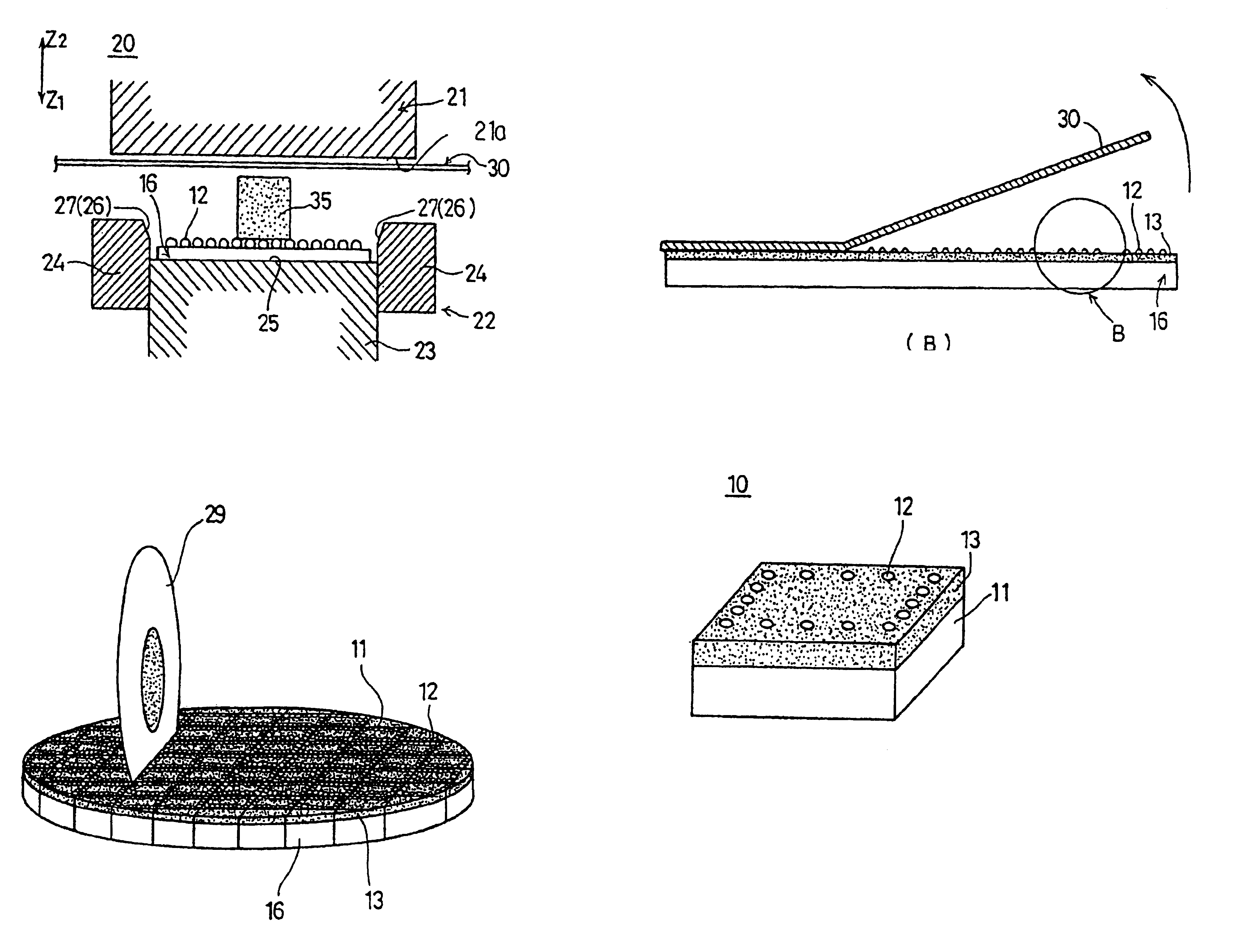
[0284]First, referring to parts (A) and (B) of FIG. 9, a description will be given of the semiconductor device 10 fabricated by the fabrication method shown in FIGS. 1 through 8 according to the present invention. The semiconductor device 10 has a very simple structure, which is generally made up of a semiconductor element 11, bumps 12 serving as protruding electrodes, and a resin layer 13.

[0285]The semiconductor element 11 (semiconductor chip) has a semiconductor substrate on which electronic circuits are formed. A large number of bumps 12 are arranged on a mount surface of the semiconductor substrate. The bumps 12 are provided by, for example, arranging semiconductor balls on the mount surface by a transfer method, and function as external connection electrodes. In the present embodiment, the bumps 12 are provided directly on electrode pads (not shown) formed on the semiconductor element 11.

[0286]The resin layer 13 (indicated by a pear-skin illustration) is formed of, for example,...

second embodiment

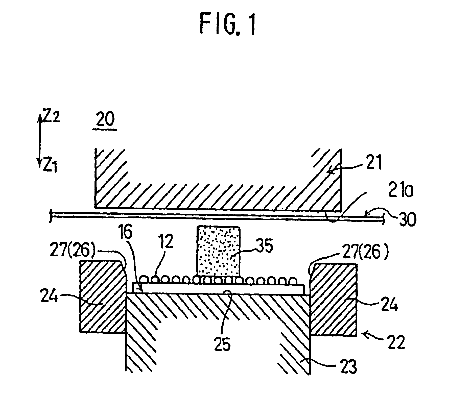
[0348]According to the present invention, the mold 20A is equipped with the excess resin removing mechanism 40. Hence, it is possible to control not only the moving speed of the upper mold 21 and the second lower mold half body 24A in the direction Z1 but also the compression pressure applied to the resin 35 using the pressure control rod 43. When the pressure control rod 43 reduces a pressure exerted in the direction Z2, the sealing resin 35 receives a reduced pressure in the cavity 28. When the pressure control rod 43 increases a pressure exerted in the direction Z2, the sealing resin 35 receives an increased pressure in the cavity 28.

[0349]For example, if the amount of the sealing resin 35 is greater than the volume of the resin layer 13 and the cavity 28 has an increased pressure due to excess resin, the resin molding may be performed appropriately. In such a case, as shown in FIG. 10(C), the pressure control rod 43 of the excess resin removing mechanism 40 is moved down in the ...

fifth embodiment

[0363]A description will now be given of a semiconductor device fabrication method according to the present invention.

[0364]FIGS. 13 and 14 show the semiconductor device fabrication method according to the fifth embodiment of the present invention. In FIGS. 13 and 14, parts that have the same structures as those of the first embodiment of the present invention which has been described with reference to FIGS. 1 through 9 are given the same reference numbers, and a description thereof will be omitted.

[0365]According to the present embodiment, as shown in FIG. 13(A), a reinforcement plate 50 is attached to the first lower mold half body 23 before the substrate 16 is loaded onto the mold 20 in the substrate loading step. The reinforcement plate 50 is made of a substance having a predetermined mechanical strength and a predetermined heat radiation performance, and is formed of, for example, an aluminum plate. The diameter of the reinforcement plate 50 is slightly greater than that of the...


PUM

PropertyMeasurementUnit
degree of freedomaaaaaaaaaa
pressureaaaaaaaaaa
heat radiating performanceaaaaaaaaaa

Abstract

A method includes a resin sealing step of placing, in a cavity 28 of a mold 20, a substrate 16 to which semiconductor elements 11 on which bumps 12 are arranged, a resin sealing step of supplying resin 35 to positions of the bumps 12 so that a resin layer 13 sealing the bumps 12 is formed, a protruding electrode exposing step of exposing at least ends of the bumps 12 sealed by the resin layer 13 so that ends of the bumps 12 are exposed from the resin layer 13, and a separating step of cutting the substrate 16 together with the resin layer 13 so that the semiconductor elements 11 are separated from each other.

Description

[0001]This application is a division of prior application Ser. No. 09 / 029,608, filed May 15, 1998, which is a §317 of international application No. PCT / JP97 / 02405, filed Jul. 10, 1997.TECHNICAL FIELD[0002]The present invention relates to a method and mold for manufacturing a semiconductor device, and a semiconductor device, and more particularly to a method and mold for manufacturing a semiconductor device having a chip-size package structure, and such a semiconductor device.[0003]Recently, there has been activity in down-sizing of semiconductor devices and increasing the integration density thereof in order to meet requirements of down-sizing of electronic devices and apparatus. A semiconductor device having a so-called chip-size package structure has been proposed in which the shape of the semiconductor device is arranged so as to be as similar to that of a semiconductor element (chip) as possible.[0004]As an increased number of pins is employed to increase the integration density...

Claims


Application Information

Patent Timeline
Patent Type & Authority Patents(United States)
IPC IPC(8): B29C43/18H01L21/56H01L25/065H01L23/495H01L23/31H01L21/68H01L23/28H01L23/498H01L23/16H01L23/24H01L23/48H01L21/67H01L21/02H01L25/10H01L21/301H01L29/06
CPCB29C43/18H01L21/56H01L21/561H01L21/563H01L21/566H01L21/568H01L23/24H01L23/3107H01L23/3114H01L23/3121H01L23/3128H01L23/49572H01L23/4985H01L24/27H01L24/97H01L25/0657H01L25/105H01L24/29B29C2043/3444B29C2043/3628H01L29/0657H01L2221/68377H01L2224/13022H01L2224/274H01L2224/48091H01L2224/73203H01L2224/73204H01L2224/83101H01L2224/83191H01L2224/85001H01L2224/97H01L2225/06517H01L2225/0652H01L2225/06527H01L2225/06541H01L2225/06551H01L2225/06572H01L2225/06579H01L2225/06582H01L2225/06586H01L2225/06589H01L2924/01005H01L2924/01013H01L2924/01029H01L2924/01046H01L2924/0105H01L2924/01074H01L2924/01078H01L2924/01079H01L2924/01082H01L2924/15174H01L2924/15192H01L2924/15311H01L2924/1532H01L2924/15331H01L2924/16195H01L2924/3011H01L2224/16225H01L2224/32225H01L24/48H01L2924/01006H01L2924/01033H01L2924/0134H01L2224/45144H01L2924/3511H01L2225/1064H01L2225/107H01L2224/29111H01L2224/92125H01L2225/1005H01L2224/16235H01L2924/00014H01L2924/00H01L2924/01028H01L2924/01051H01L2924/3512H01L2924/181H01L24/45H01L2224/73104H01L2224/02371H01L2224/04105H01L2224/13024H01L2924/15184H01L2924/1815H01L2924/18161H01L2224/05599H01L2924/00012
Inventor FUKASAWA, NORIOKAWAHARA, TOSHIMIMORIOKA, MUNEHARUOSAWA, MITSUNADASHINMA, YASUHIROMATSUKI, HIROHISAONODERA, MASANORIKASAI, JUNICHIMARUYAMA, SHIGEYUKISAKUMA, MASAOSUZUKI, YOSHIMITAKENAKA, MASASHI
Owner SOCIONEXT INC
Why Eureka
Try Eureka