Process and unit for production of polycrystalline silicon film

a polycrystalline silicon and film technology, applied in the direction of manufacturing tools, instruments, non-linear optics, etc., can solve the problems of low performance of thin film transistors, low efficiency, and difficulty in fabricating integrated circuits where high speed and high performance are required, and achieve low cost, high productivity, and efficient production

Inactive Publication Date: 2005-04-26
MITSUBISHI ELECTRIC CORP +1
View PDF12 Cites 33 Cited by
  • Summary
  • Abstract
  • Description
  • Claims
  • Application Information

AI Technical Summary

Benefits of technology

[0017]Furthermore, the laser, of which the wavelength is in the above described range, has a large absorption coefficient with respect to amorphous silicon while the absorption ratio with respect to polycrystal silicon is small and, therefore, the amorphous silicon is converted to a polycrystal silicon through the first irradiation and, then, no characteristics are changed due to the second irradiation in the portion that is twice irradiated with the laser. Therefore, there is no difference in the characteristics between the portion irradiated with the laser once and the portion irradiated with the laser twice so that a high quality polycrystal silicon film can be provided.
[0036]In addition, a semiconductor device according to this invention uses a polycrystal silicon film produced by means of the above described process as an active region. In this case, since a polycrystal silicon film of which the mobility is large and of which the area is large is used as an active region, a semiconductor device of which the area is large and that is of high performance can be provided

Problems solved by technology

At present, however, the crystallinity of the silicon film that forms an active layer of transistors is poor and, therefore, the performance of thin film transistors, represented by mobility, is low and it is difficult to fabricate an integrated circuit wherein high speed and high performance are required.
Crystal defects locate in crystal grain boundaries of the polycrystal silicon and they block the carrier movement in the active layer of the thin film transistors.
As a result, a high speed of operation of the transistors is difficult so that it is difficult to achieve a high response of the liquid crystal display device.
Therefore, the manufacturing of a polycrystalline silicon film for manufacturing a liquid crystal display having a large area is difficult.

Method used


Image

  • Process and unit for production of polycrystalline silicon film
  • Process and unit for production of polycrystalline silicon film
  • Process and unit for production of polycrystalline silicon film

Examples


first embodiment

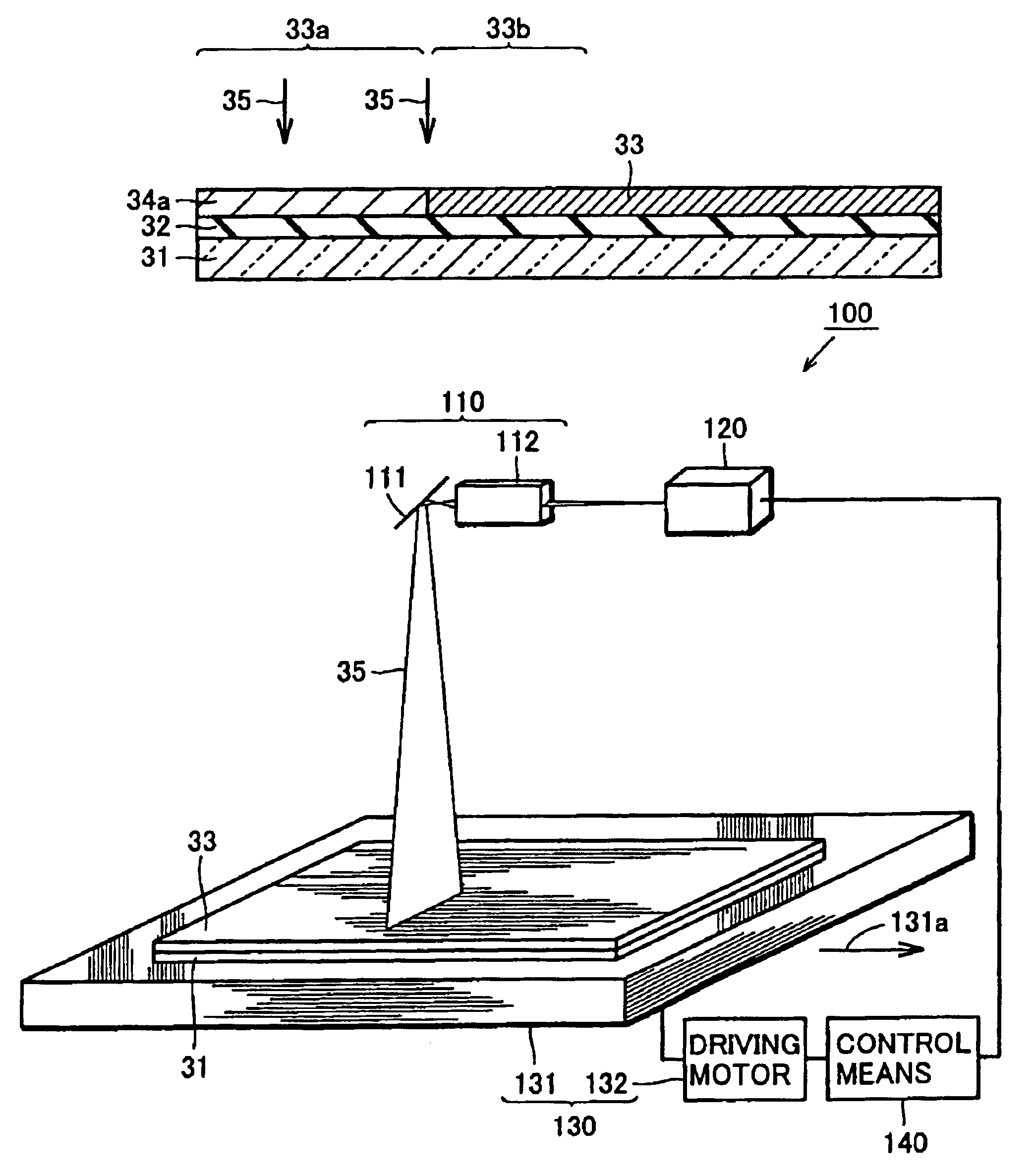
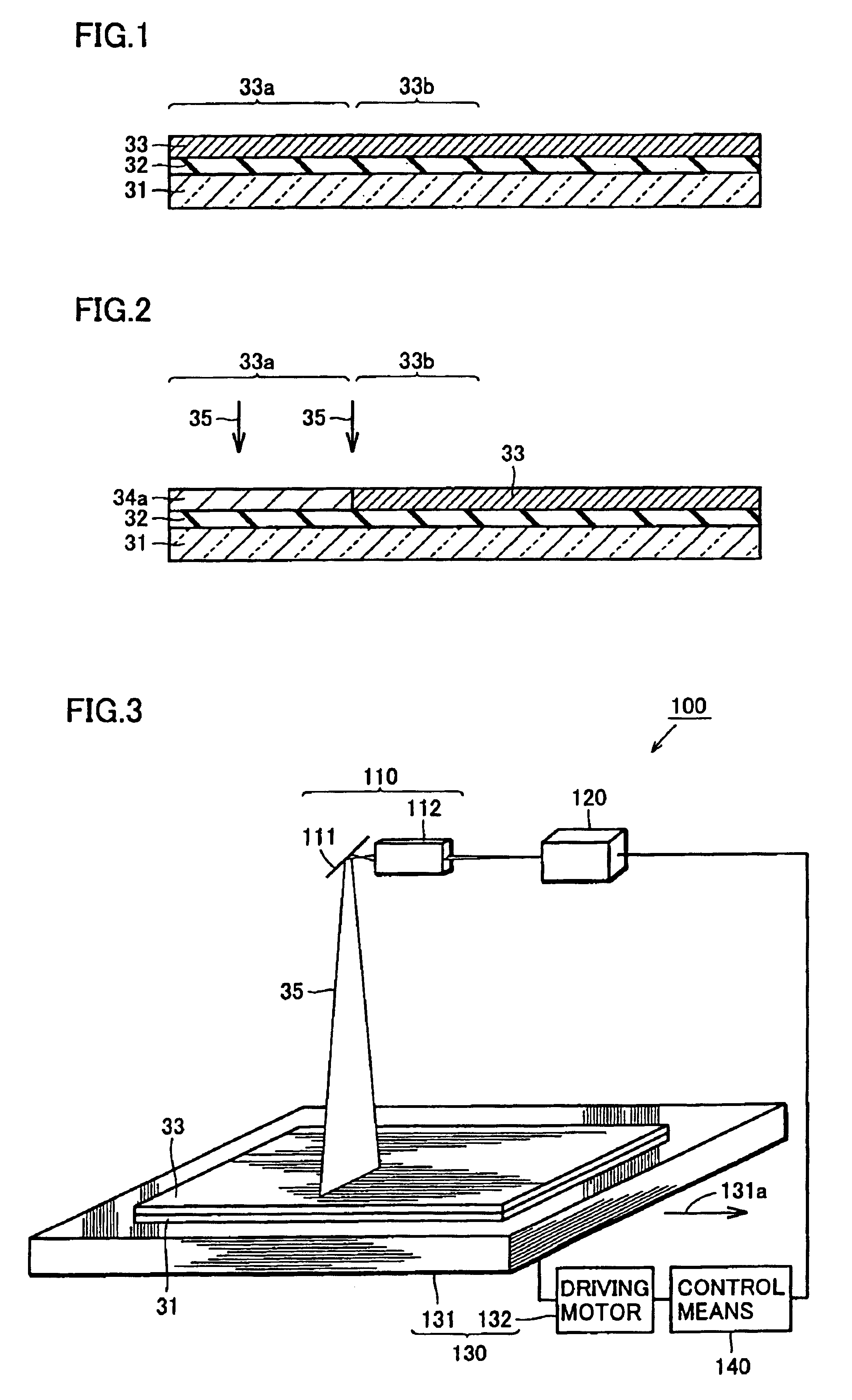
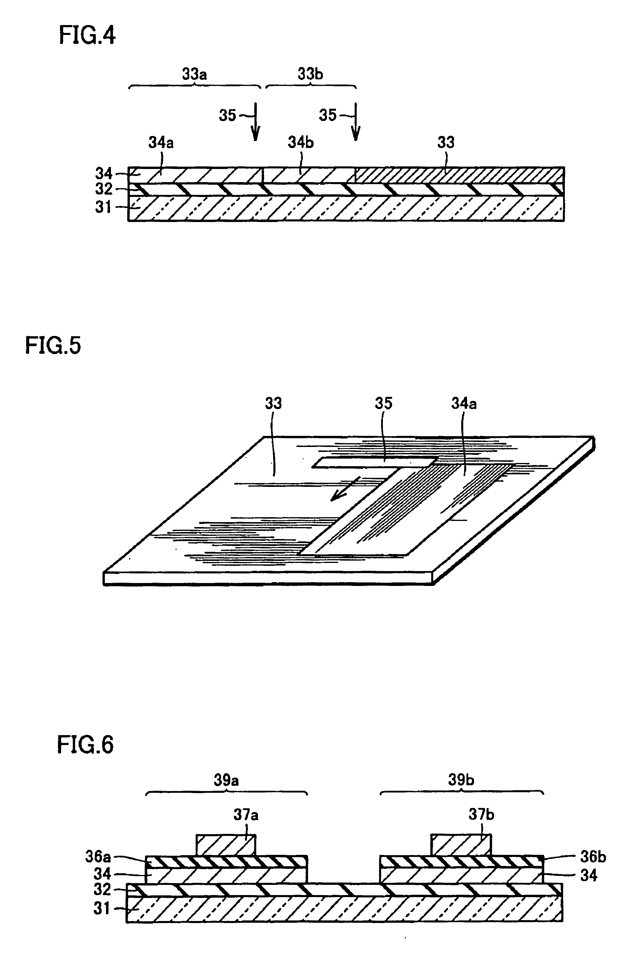
[0057]FIGS. 1 to 6 are views showing a process for a polycrystal silicon film according to a first embodiment of this invention. Referring to FIG. 1, a silicon oxide film 32 is formed on a glass substrate 31 by means of, for example, a CVD method. An amorphous silicon film 33 is formed on silicon oxide film 32 by means of a CVD method. This amorphous silicon film 33 has a first region 33a and a second region 33b that contacts this first region 33a.

[0058]Referring to FIGS. 2 and 3, first region 33a of amorphous silicon film 33 is irradiated with the second harmonics laser (wavelength 532 nm) of Nd: YAG of the Q switch. Thereby, a portion irradiated with a laser 35 is polycrystallized so as to form a first polycrystal portion 34a. At this time, a unit, as shown in FIG. 3, is used for the irradiation by the laser.

[0059]Referring to FIG. 3, a polycrystal silicon film production unit 100 is provided with a laser oscillator 120 as an oscillation means for oscillating a laser of which the...

second embodiment

[0084]FIG. 13 is a perspective view showing a process for a polycrystal silicon film according to a second embodiment of this invention. The irradiation means of a polycrystal silicon film production unit 180, shown in FIG. 13, differs from that of the polycrystal silicon film production unit 100. That is to say, in the polycrystal silicon film production unit 180, shown in FIG. 13, a first irradiation means 110a, a second irradiation means 110b and a third irradiation means 110c exist as the irradiation means. First, second and third irradiation means 110a, 110b and 110c are, respectively, formed of a mirror 111 and a beam formation optical system 112. Mirror 111 and beam formation optical system 112 are similar to those shown in FIG. 3. A laser oscillator 120a, as the first oscillation means, a laser oscillator 120b as the second oscillation means and a laser oscillator 120c as the third oscillation means are connected to respective beam formation optical systems 112. Laser oscill...

third embodiment

[0091]FIG. 17 is a perspective view of a production unit for a polycrystal silicon film according to a third embodiment of this invention. Referring to FIG. 17, a polycrystal silicon film production unit 190 according to the third embodiment differs from that of other embodiments in the point that a laser oscillated from one laser oscillator 420 is used by three irradiation means. That is to say, the irradiation means has a first irradiation means 210a, a second irradiation means 210b and a third irradiation means 210c. Irradiation means 210a, 210b and 210c have, respectively, a beam formation optical system 112 and a mirror 111 that are the same as those in the first embodiment. The mirror 114 reflects a laser that is oscillated by laser oscillator 420 of which the wavelength is not less than 390 nm and not more than 640 nm so that amorphous silicon film 33 is irradiated with this laser in the form of lasers 35a, 35b and 35c via beam formation optical systems 112 and mirrors 111. T...


PUM

PropertyMeasurementUnit
wavelengthaaaaaaaaaa

Abstract

A process for making a polycrystalline silicon film includes forming, on a glass substrate, an amorphous silicon film having a first region and a second region that contacts the first region, forming a first polycrystalline portion by irradiating the first region of the amorphous silicon film with laser light having a wavelength not less than 390 nm and not more than 640 nm and forming a second polycrystalline portion that contacts the first polycrystalline portion by irradiating the second region and the portion of the region of the first polycrystalline portion that contacts the second region of the amorphous silicon film with the laser light.

Description

TECHNICAL FIELD[0001]The present invention relates to a process and a unit for production of a polycrystalline silicon film as well as a semiconductor device and a process for the same, in particular, to a process and a unit for production of a polycrystalline silicon film with excellent crystallinity, for making a thin film transistor, having high carrier mobility as a semiconductor device, and a process for the making the semiconductor device and in which the polycrystalline silicon film is used.BACKGROUND ART[0002]At present, the pixel part of a liquid crystal panel forms images through switching of thin film transistors fabricated with an amorphous or polycrystal silicon film on a substrate of glass or synthesized quartz. In the case that it becomes possible to simultaneously form a driver circuit (at present mainly installed independently outside of the panel) to drive pixel transistors on this panel, there would be great merit with respect to production cost, reliability, and ...

Claims


Application Information

Patent Timeline
Patent Type & Authority Patents(United States)
IPC IPC(8): H01L21/02H01L21/20H01L21/336C23C14/58
CPCB23K26/0838C23C14/5813H01L21/02532H01L21/02691H01L29/66757H01L21/02678Y10S438/969B23K26/0604B23K26/0738B23K26/352B23K2101/40B23K2103/52G02F1/13
Inventor OGAWA, TETSUYATOKIOKA, HIDETADANISHIMAE, JUNICHIOKAMOTO, TATSUKISATO, YUKIOINOUE, MITSUOMIYASAKA, MITSUTOSHIJIROKU, HIROAKI
Owner MITSUBISHI ELECTRIC CORP
Why Eureka
Try Eureka