Manufacturing method of semiconductor device and substrate processing apparatus

a manufacturing method and substrate technology, applied in the direction of coatings, chemical vapor deposition coatings, metallic material coating processes, etc., can solve the problems of difficult to obtain difficult to achieve the thin film deposited by the mocvd method, etc., to improve the flatness of the thin film without lowering productivity

Inactive Publication Date: 2005-04-26
KOKUSA ELECTRIC CO LTD
View PDF10 Cites 50 Cited by
  • Summary
  • Abstract
  • Description
  • Claims
  • Application Information

AI Technical Summary

Benefits of technology

[0029]It is an object of the present invention to provide a manufacturing method of a semiconductor device and a substrate processing apparatus which can improve flatness of a thin film without generating particles. It is another object of the present invention to provide a manufacturing method of a semiconductor device which can improve the flatness of the thin film without lowering productivity.

Problems solved by technology

Incidentally, there is a problem that it is difficult for the thin film deposited by the aforementioned MOCVD method to obtain flatness of the film surface.
Particularly, the problem described above becomes remarkable in the MOVCD method in which the deposition rate of the thin film is determined by the surface-reaction rate controlling.
Therefore, it is difficult for the thin film deposited by the MOCVD method to obtain flatness of the surface of the thin film 32 as shown in FIG.
This flatness of the surface of the thin film 32 is a factor to lower the reliability of the semiconductor device which is an end product and produces a big problem with downsizing of the device.
However, there are following problems in the above-described publicly known examples.

Method used


Image

  • Manufacturing method of semiconductor device and substrate processing apparatus
  • Manufacturing method of semiconductor device and substrate processing apparatus
  • Manufacturing method of semiconductor device and substrate processing apparatus

Examples


first embodiment

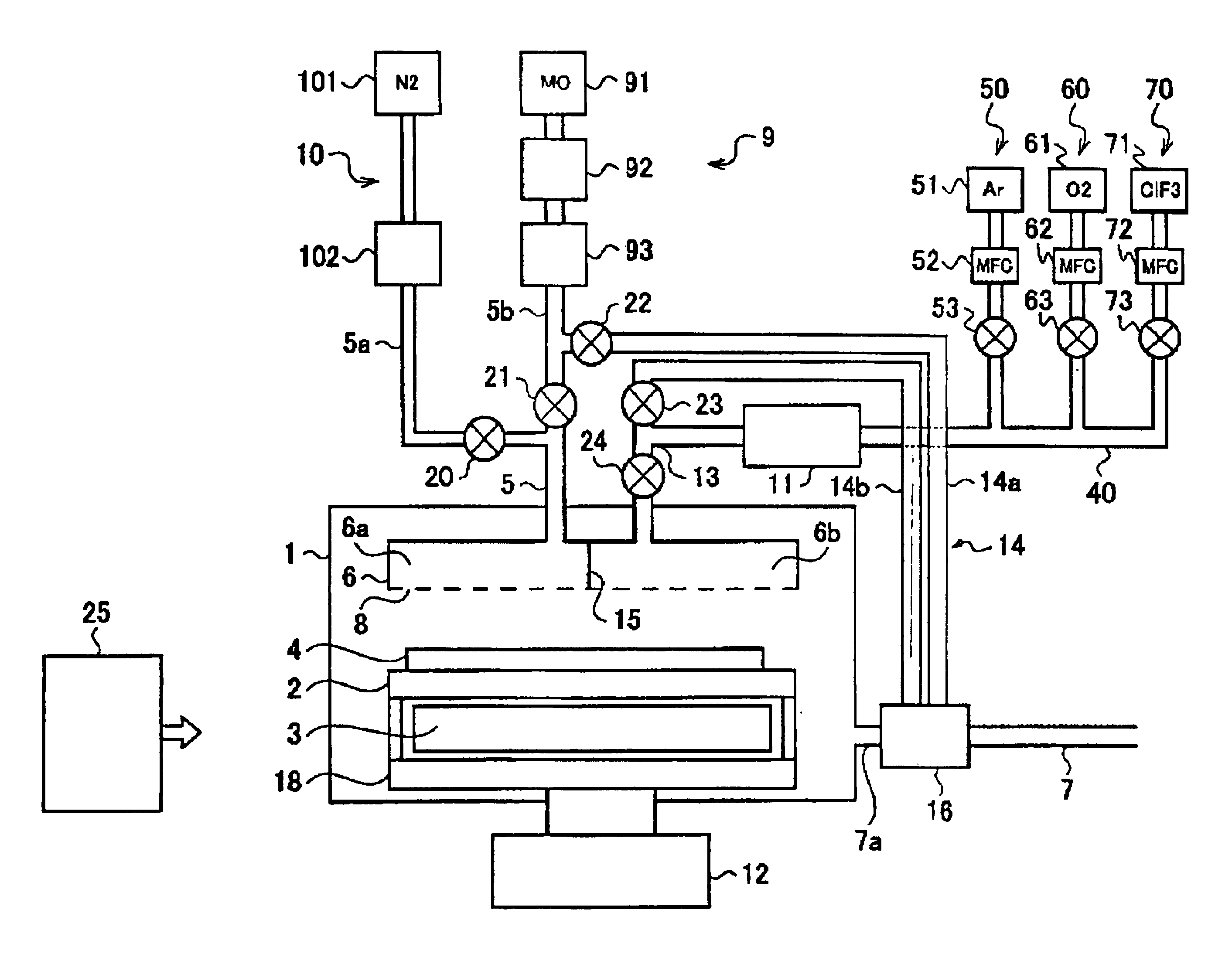
[0099]FIG. 9 is a schematic view showing an example of a single wafer type CVD apparatus which is a substrate processing apparatus relating to the embodiments. A radical generating unit 11, a substrate rotating unit 12, an inert gas supply unit 10 and bypass pipes 14 are mainly added to a conventional reaction chamber 1 (FIG. 10).

[0100]A hollow heater unit 18 whose upper opening is covered with a susceptor 2 is provided in the reaction chamber 1 as shown in FIG. 9. A heater 3 is provided in the heater unit 18 and the heater 3 is adapted to heat a substrate 4 mounted on the susceptor 2 to a predetermined temperature. The substrate 4 mounted on the susceptor 2 is, for example, a semiconductor silicon wafer, a glass substrate, or the like.

[0101]The substrate rotating unit 12 is provided outside the reaction chamber 1 and the substrate 4 on the susceptor 2 can be rotated by rotating the heater unit 18 in the reaction chamber 1. The substrate 4 is rotated so that a source gas introduced ...

second embodiment

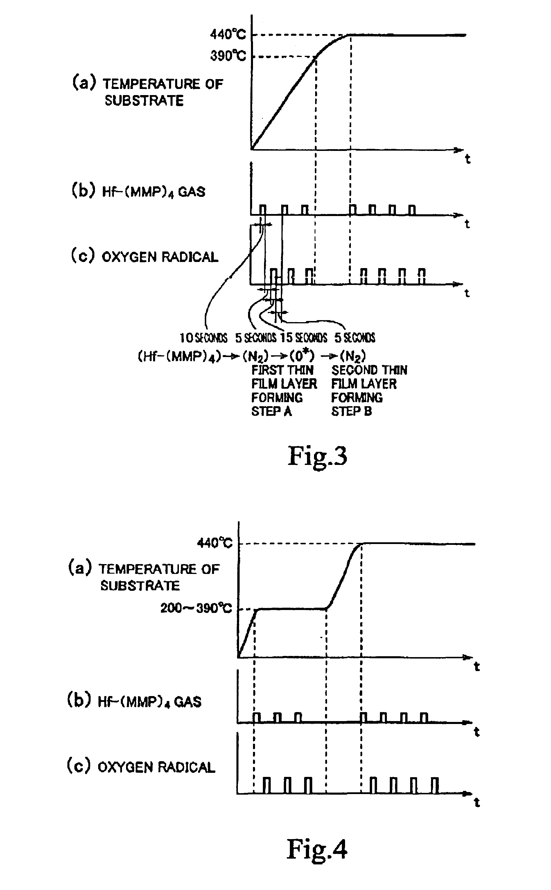
[0163]Incidentally, though the first thin film layer is formed while the temperature is raised in the above-described process timing according to the first embodiment in FIG. 3, the first thin film layer may be formed not while the temperature is raised but while a predetermined low temperature (at least 200° C. no more than 390° C.) is kept. FIG. 4(a) to FIG. 4(c) show a timing chart of the process of the second embodiment in which the first thin film layer forming step [the supply of the source gas→the supply of the oxygen radical] is repeated for n cycles in a condition that such a low temperature is kept. FIG. 4(a) shows a property of raising temperature of the substrate, in which a horizontal axis indicates time and a vertical axis indicates temperature. FIG. 4(b) shows a timing of supplying the Hf-(MMP)4 source gas and FIG. 4(c) shows a timing of supplying the oxygen radical respectively, in which a horizontal axis indicates time and a vertical axis indicates a supply amount (...

third embodiment

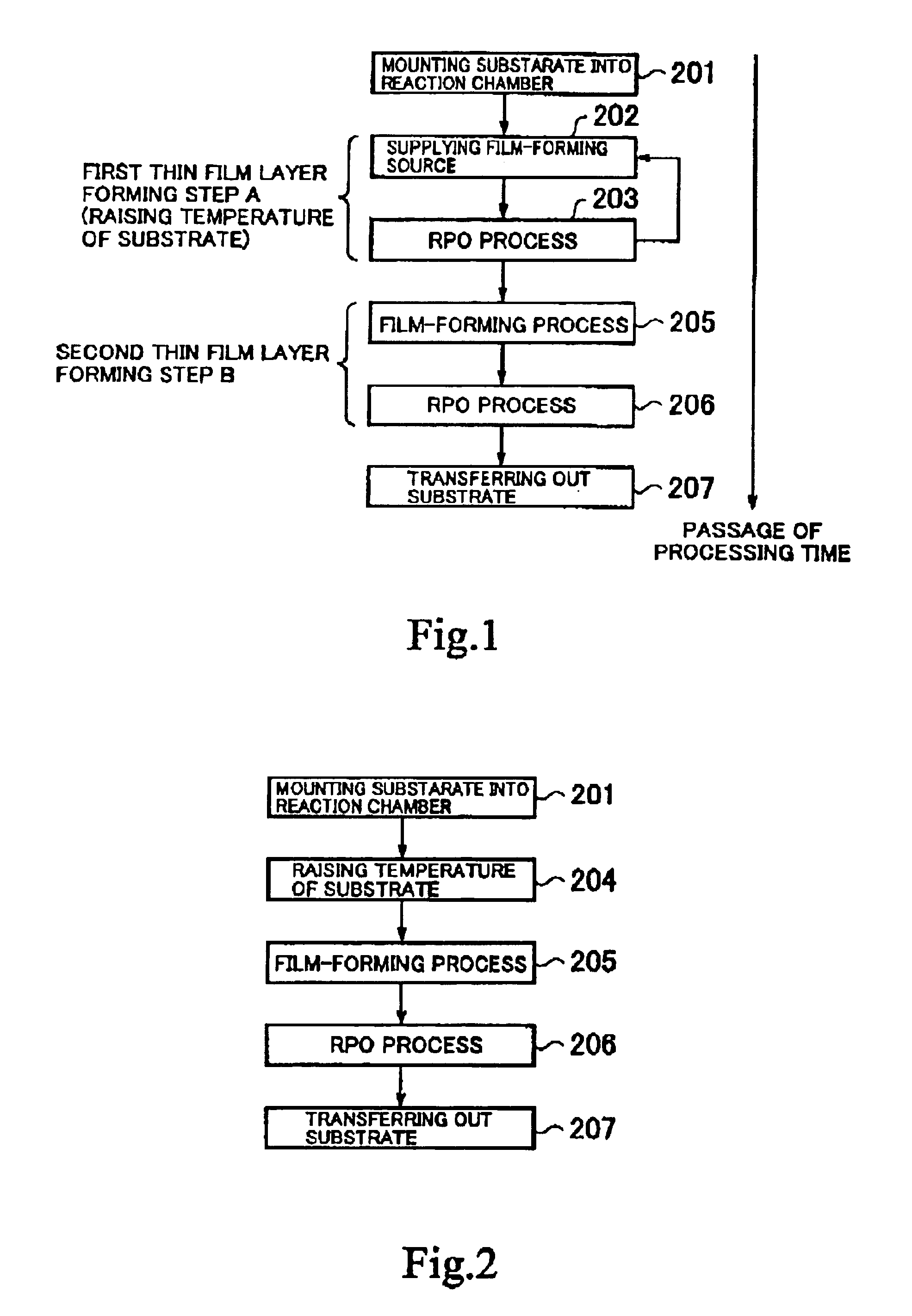
[0167]FIG. 11 shows a process flow according to a third embodiment. As shown in this drawing, in this embodiment, a film is formed in such a manner that a step of making a source gas adhere onto a substrate (step 202) and a step of forming a film (HfO2 film) by supplying onto the substrate a reactant which is obtained by plasma activation of a gas containing an oxygen atom (step 203) are repeated a plurality of times in this order during a period from the transfer of the substrate into a reaction chamber (step 201) to the transfer of the substrate out of the reaction chamber (step 207). In other words, the second thin film layer forming step is not performed in this embodiment, and n cycles of [the film-forming source supply (step 202)→the RPO process (step 203)] are repeated from the beginning to the end, thereby forming the film. Here, the film-forming source supply (step 202) and the RPO process (step 203) are performed in this order so that such an effect is obtainable that EOT ...


PUM

PropertyMeasurementUnit
temperatureaaaaaaaaaa

Abstract

According to the present invention, flatness of a thin film formed on a substrate is improved without generating particles and lowering productivity. A method of manufacturing a semiconductor device includes a first thin film layer forming step A and a second thin film layer forming step B. In the first thin film layer forming step A, on the way of heating and raising the temperature of the substrate up to a film-forming temperature, a film-forming source supply in which an organic source gas is made adhere onto the substrate in yet unreacted state is performed (202), and thereafter, a RPO process (Remote Plasma Oxidation) in which an oxygen radical is supplied onto the substrate to form a first thin film layer is performed (203). In this first thin film layer forming step A, it is preferable to repeat the film-forming source supply onto the substrate and the RPO process more than once. In the second thin film layer forming step B, after the source gas is supplied onto the substrate by a thermal CVD method to perform a film-forming process (205) after raising the temperature of the substrate to the film-forming temperature, the RPO process is performed to form a second thin film layer on the first thin film layer with a predetermined film thickness (206).

Description

BACKGROUND OF THE INVENTION[0001]1. Field of the Invention[0002]The present invention relates to a manufacturing method of a semiconductor device and a substrate processing apparatus in which a thin film is formed on a substrate.[0003]2. Description of the Related Art[0004]As one of manufacturing steps of a semiconductor, there is a CVD (Chemical Vapor Deposition) step in which a predetermined film-forming process is preformed on a surface of a substrate (a substrate to be processed based on a silicon wafer, glass, or the like, on which a fine electric circuit pattern is formed). In this step, the substrate is mounted in an airtight reaction chamber and heated by a beater provided in the chamber, and chemical reaction is caused while introducing a source gas to the substrate so as to form a thin film evenly on the fine electric circuit pattern formed on the substrate. In this reaction chamber, a thin film is also formed on components other than the substrate. A CVD apparatus shown i...

Claims


Application Information

Patent Timeline
Patent Type & Authority Patents(United States)
IPC IPC(8): C23C16/458C23C16/40C23C16/52C23C16/448C23C16/44C23C16/452H01L21/02H01L21/316H01L21/31C23C16/455
CPCC23C16/405C23C16/4405C23C16/452C23C16/45527H01L21/31604C23C16/45574C23C16/4584C23C16/52C23C16/45565H01L21/022H01L21/0228H01L21/02252
Inventor ASAI, MASAYUKIKITAYAMA, KANAKO
Owner KOKUSA ELECTRIC CO LTD
Why Eureka
Try Eureka