High resolution tiled microchannel storage phosphor based radiation sensor

a radiation sensor and high-resolution technology, applied in the field of xray imaging screens, can solve the problems of loss of spatial resolution and contrast in images, grainy images, etc., and achieve the effect of increasing resolution, high resolution and ensuring accuracy

Inactive Publication Date: 2005-04-26
NANOCRYSTAL IMAGING
View PDF7 Cites 17 Cited by
  • Summary
  • Abstract
  • Description
  • Claims
  • Application Information

AI Technical Summary

Benefits of technology

[0008]Many processes for producing microchannel imaging plates are limited by the largest dimension of the plate that can be readily produced. Many otherwise suitable processes produce plates that have a maximum dimension of 2 to 4 inches. However, many X-ray imaging applications require plates of larger sizes. Larger size plates can be manufactured by combining a number of smaller plates by “tiling” or forming a mosaic of smaller plates. However, simply arranging smaller plates on a base substrate can make it very difficult to repair a damaged imaging screen even if only a small portion of the overall plate is damaged. The present invention provides an improved construction for imaging screens formed from a plurality of tiled microchannel plates.
[0009]Recently a new type of phosphor has been utilized in X-ray imaging screens, this phosphor is known as a “storage phosphor” or “photostimulable storage phosphor”. Screens comprised of storage phosphors may used in place of standard scintillator or film plates in X-ray imaging systems. After exposure to X-rays the storage phosphors will retain the X-ray image for a significant period of time so that the image can be read out at a remote location long after the image has been “exposed”. The image is read out by thermal or optical stimulation such as by scanning with a laser. After readout of the stored image, the imaging screen is then “reset” for subsequent reuse. These storage phosphor screens are very suitable for computerized radiography applications. However, previous storage phosphor imaging s

Problems solved by technology

In particular, light scattering by the phosphor particles and their grain boundaries results in loss of spatial resolution and contrast in the image.
As the light diffuses, it spreads out which results in a loss of spatial resolution and contrast in the image.
However, use of the standard larger-particle phosphors in thin screens results in grainy images, poor resolution and low X-ray absorption.
Many processes for producing microchannel imaging plates are limited by the largest dimension of the plate that can be readily produced.
However, simply arranging smaller plates on a base substrat

Method used


Image

  • High resolution tiled microchannel storage phosphor based radiation sensor
  • High resolution tiled microchannel storage phosphor based radiation sensor
  • High resolution tiled microchannel storage phosphor based radiation sensor

Examples


Embodiment Construction

[0028]Basic Construction

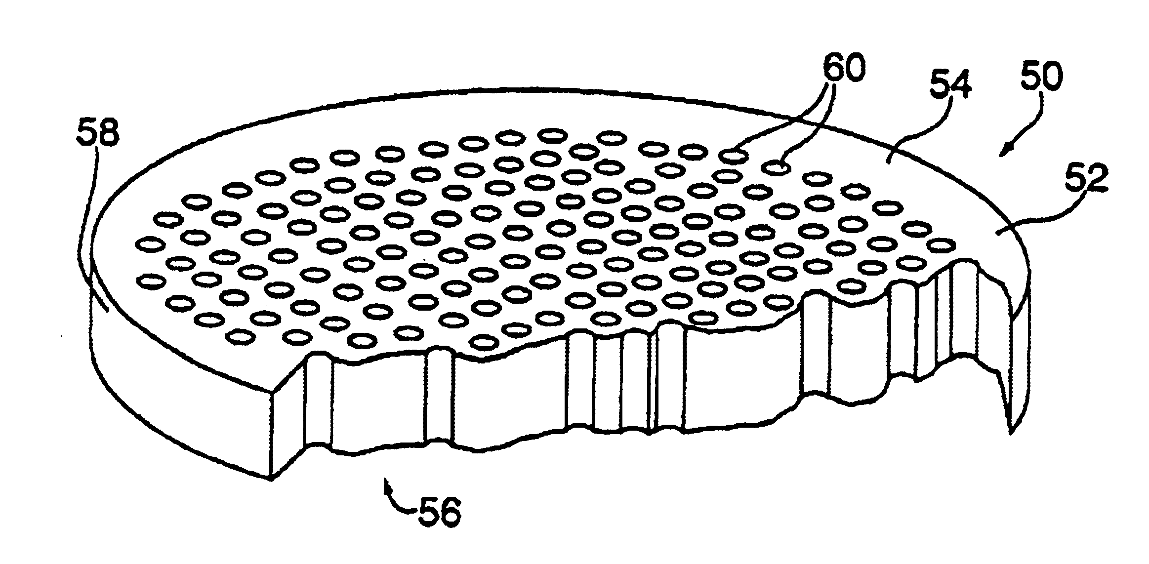
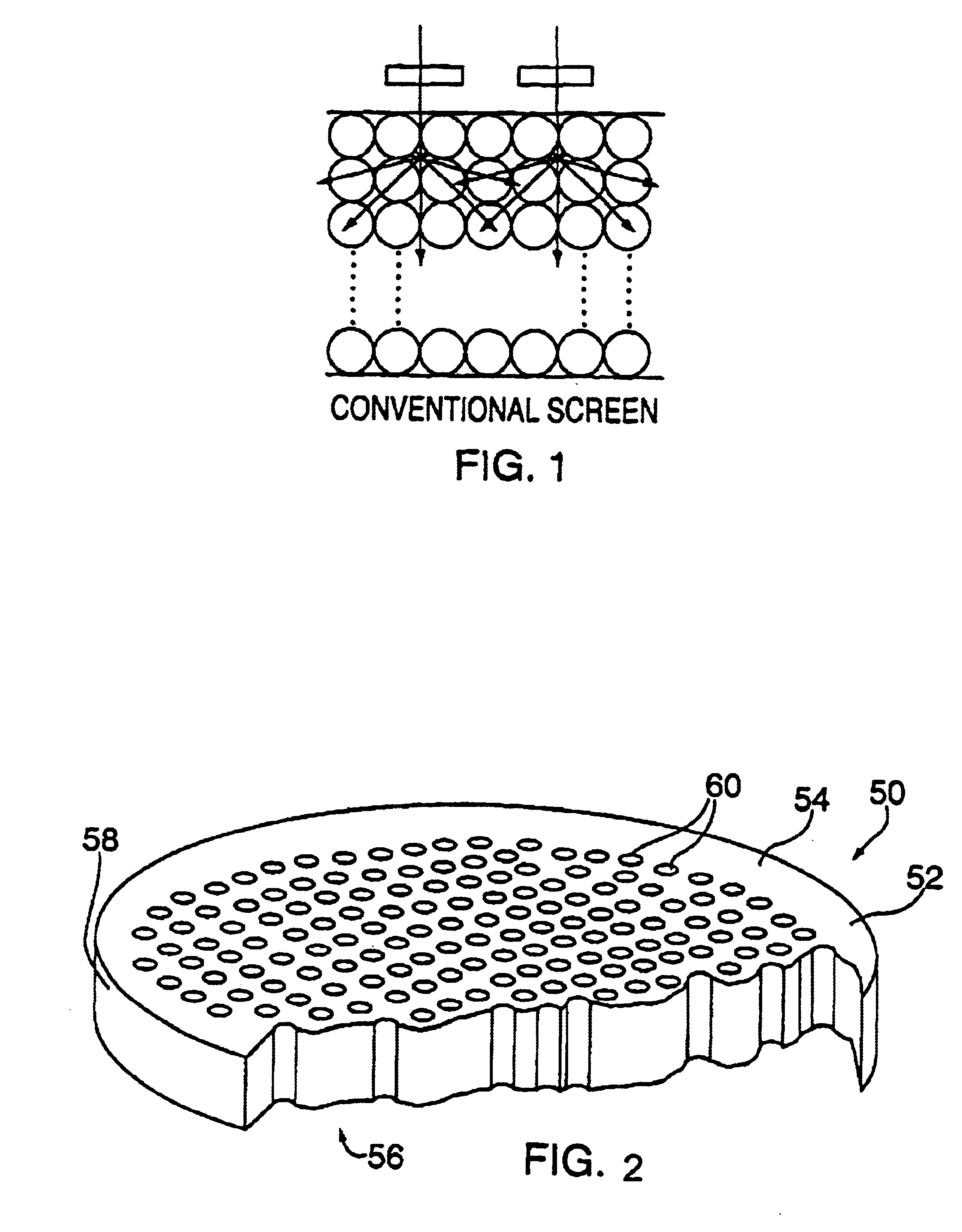
[0029]FIG. 2 illustrates a microchannel phosphor screen 50 for converting radiation impinging thereon to visible light which has use, for example in an X-ray imaging system. Microchannel phosphor screen 50 comprises a substrate 52 which has an upper planar surface 54, a lower planar surface 56 and a cylindrical edge 58. Extending from upper surface 54 to lower surface 56 of substrate 52 are a multiplicity of small channels (“microchannels”) 60 which have a diameter on the order of about 0.5-40μ (microns) and more usually 5-20μ. Microchannels 60 are spaced apart approximately 1 to 12 microns, and the plate has a thickness on the order of 50-2000 microns (which is also the length of the microchannels). The material used as the substrate can be glass, silicon (crystalline, alpha, amorphous, or polysilicon as used in the fabrication of integrated circuits) as well as metals such as aluminum as techniques for the micro formation of microchannels exist for all of t...


PUM


Abstract

X-ray imaging screens utilizing phosphors disposed in microchannels disposed in a plate. This application relates to the “tiling” of such microchannel plates to form a larger imaging area and to the use of “storage phosphors” in the microchannel plates which enables the phosphors to be read out after exposure and from the side exposed to the X-rays. The storage phosphor screens of the present invention provide significantly increased resolution than the prior art storage phosphor screens.

Description

CLAIM FOR PRIORITY[0001]This application claims the priority of U.S. Provisional patent application Ser. No. 60 / 268,137 filed Feb. 12, 2001, entitled “High Resolution Tiled Microchannel Storage Phosphor Based Radiation Sensor”REFERENCE TO RELATED APPLICATIONS[0002]This application is a continuation in part of U.S. patent application Ser. No. 09 / 688,662 filed Oct. 16, 2000 now U.S. Pat. No. 6,534,772 Entitled “High Resolution High Output Microchannel Based Radiation Sensor” which is a continuation in part of U.S. patent application Ser. No. 09 / 385,995 filed Aug. 30, 1999 now U.S. Pat. No. 6,452,184 Entitled “Microchannel High Resolution X-ray Sensor Having an Integrated Photomultiplier” which is a continuation in part of U.S. patent application Ser. No. 09 / 197,248 filed Nov. 20, 1998 now U.S. Pat. No. 6,300,640 Entitled “Composite Nanophosphor Screen For Detecting Radiation Having Optically Reflective Coatings” which in turn is a continuation in part of Ser. No. 08 / 980,416 filed Nov....

Claims


Application Information

Patent Timeline
IPC IPC(8): G01T1/20G01T1/29G01T1/00G21K4/00
CPCG01T1/20G01T1/2921G21K4/00H01J2231/5016G21K2004/12H01J2231/50036G21K2004/06
Inventor TASKAR, NIKHIL R.SHARGAVA, RAMESHWAR NATH
Owner NANOCRYSTAL IMAGING
Why Eureka
Try Eureka