Gettering technique for wafers made using a controlled cleaving process

Inactive Publication Date: 2005-05-10
SILICON GENERAL CORPORATION
View PDF250 Cites 79 Cited by
  • Summary
  • Abstract
  • Description
  • Claims
  • Application Information

AI Technical Summary

Benefits of technology

[0009]According to the present invention, a technique including a method and device for removing impurities from an SOI wafer made using a controlled cleaving process is provided. In an exemplary embodiment, the present invention provides an SOI wafer with a gettering layer for removing impurities from an active

Problems solved by technology

These techniques, however, are not free from limitations.
For example, conventional isolation techniques consume a considerable amount of valuable wafer surface area on the chip, and often generate a non-planar surface as an artifact of the isolation process.
Either or both of these considerations generally limit the degree of integration achievable in a given chip.
However, many problems that have already been solved regarding fabricating devices on bulk silicon wafers remain to be solved for fabricating devices on

Method used


Image

  • Gettering technique for wafers made using a controlled cleaving process
  • Gettering technique for wafers made using a controlled cleaving process
  • Gettering technique for wafers made using a controlled cleaving process

Examples


Embodiment Construction

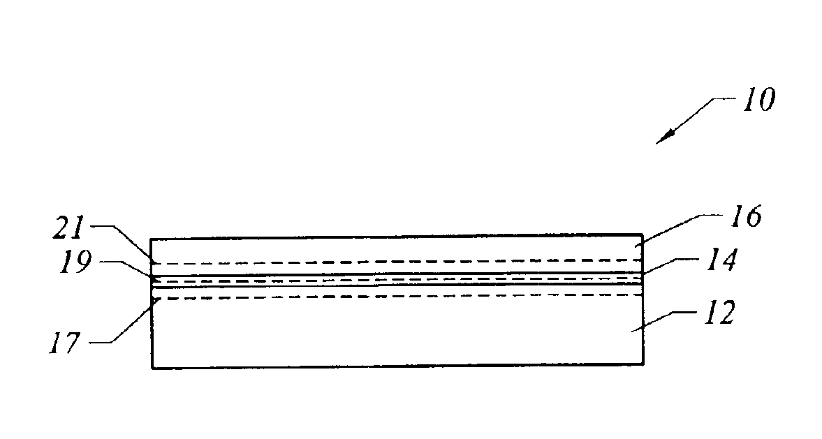
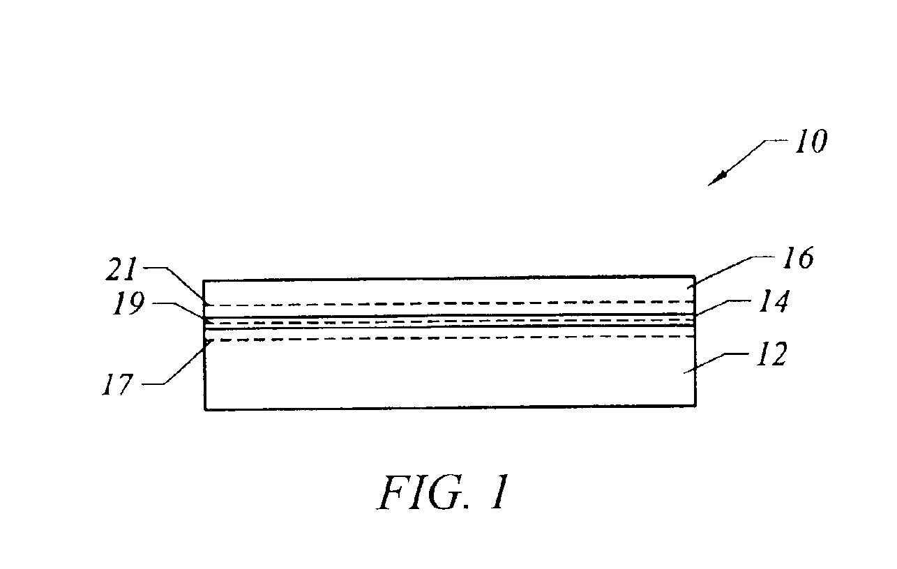
[0016]The present invention provides an SOI wafer with a gettering layer for removing impurities from an active region of an integrated circuit to be formed on the wafer. In a specific embodiment, a gettering layer is formed in an SOI wafer made using a controlled cleaving process. The gettering layer is generally beneath an active region of the devices that will be formed on the SOI wafer. The SOI wafer is made using a controlled cleaving process, which is described in Henley, noted above.

[0017]1. Silicon on Insulator Substrate

[0018]FIG. 1 is a simplified cross section of an SOI wafer 10 according to an embodiment of the present invention. The Fig. is not to scale and is merely an illustration, which should not limit the scope of the claims herein. The SOI wafer 10 includes numerous features including a lower substrate 12, an insulating layer(s) 14, and a film of material 16, which will include active devices in later processing steps. The film of material, which can be a silicon m...


PUM


Abstract

A technique for forming a gettering layer in a wafer made using a controlled cleaving process. The gettering layer can be made by implanting using beam line or plasma immersion ion implantaion, or made by forming a film of material such as polysilicon by way of chemical vapor deposition. A controlled cleaving process is used to form the wafer, which is a multilayered silicon on insulator substrate. The gettering layer removes and/or attracts impurities in the wafer, which can be detrimental to the functionality and reliability of an integrated circuit device made on the wafer.

Description

CROSS REFERENCE TO RELATED APPLICATIONS[0001]This application claims priority from the provisional patent application entitled GETTERING TECHNIQUE FOR WAFERS MADE USING A CONTROLLED CLEAVING PROCESS, filed Jul. 18, 1997 and assigned Application No. 60 / 059,980.BACKGROUND OF THE INVENTION[0002]The present invention relates to the manufacture of integrated circuits. More particularly, the present invention provides a technique for forming a gettering layer in a silicon-on-insulator wafer made using a controlled cleaving process, for example.[0003]Integrated circuits are fabricated on chips of semiconductor material. These integrated circuits often contain thousands, or even millions, of transistors and other devices. In particular, it is desirable to put as many transistors as possible within a given area of semiconductor because more transistors typically provide greater functionality, and a smaller chip means more chips per wafer and lower costs.[0004]Some integrated circuits are fab...

Claims


Application Information

Patent Timeline
IPC IPC(8): H01L21/762H01L21/02H01L21/70H01L21/322H01L21/265H01L21/20H01L21/223
CPCH01L21/76254H01L21/3223H01L21/3226H01L21/2007H01L21/2236H01L21/26506H01L21/2658
Inventor HENLEY, FRANCOIS J.CHEUNG, NATHAN W.
Owner SILICON GENERAL CORPORATION
Why Eureka
Try Eureka