Thermal processing system

Inactive Publication Date: 2005-05-10
TOKYO ELECTRON LTD
View PDF12 Cites 25 Cited by
  • Summary
  • Abstract
  • Description
  • Claims
  • Application Information

AI Technical Summary

Benefits of technology

[0023]The present invention has been devised in consideration of the above-described problems, and, an object of the present invention is

Problems solved by technology

However, this system has a configuration such that a gate valve 26 is provided in the side wall of the processing chamber 2 for bringing in the wafer W. Accordingly, there is not a necessarily sufficient isotropy in view of temperature.
As a result, it may not be possible to achieve a sufficiently uniform temperature distribution throughout the surface of the wafer W.
Further, this problem of adherence of a deposition film or a reaction by-product may also occur for the inner wall of the processing chamber 2 as it has a high temperature.
As a result, the heat capacity thereof is large, and, thereby, controllability of the temperature of the wafer W therethrough is degraded.
As a result, the directivity of t

Method used


Image

  • Thermal processing system
  • Thermal processing system
  • Thermal processing system

Examples


Embodiment Construction

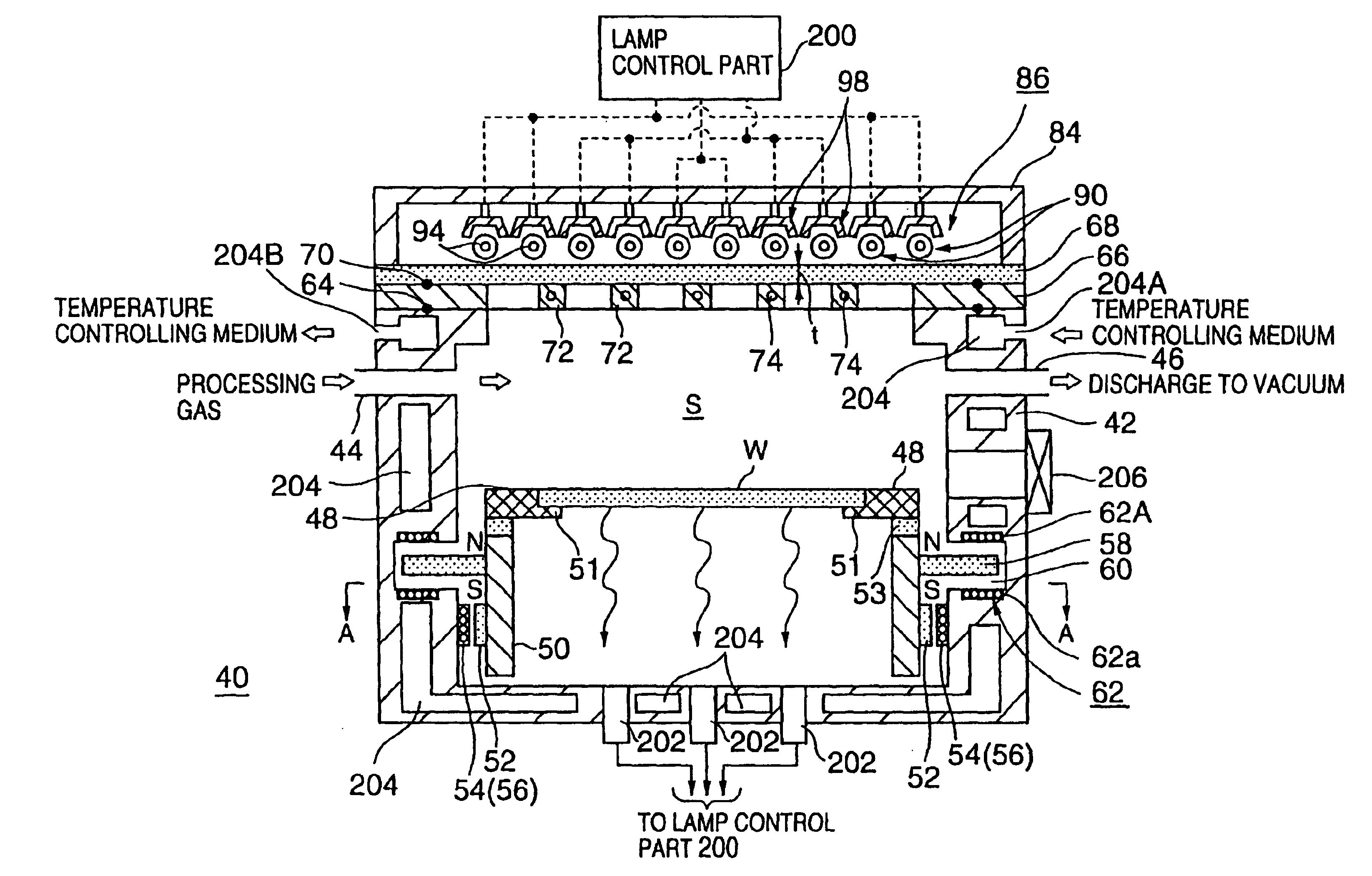
[0053]A thermal processing system in one embodiment of the present invention will now be described.

[0054]FIG. 9 shows a configuration of the thermal processing system in the embodiment of the present invention, and FIG. 10 shows a cross-sectional view of the same thermal processing system taken along a line A—A shown in FIG. 9. FIG. 11 shows a plan view of a supporting frame member, and FIG. 12 shows a plan view indicating an arrangement of tube-shaped heating lamps.

[0055]As shown in the figures, this thermal processing system 40 includes a processing chamber 42 formed to be like a cylinder from stainless steel, aluminum, or the like, for example. In a side wall of the processing chamber 42 near the top thereof, a processing gas nozzle 44 for supplying a necessary processing gas into the processing chamber 42 is provided, and, a discharge mouth 46 is provided in the side wall of the processing chamber 42 opposite to the above-mentioned nozzle 44. To the mouth 46, a vacuum pump or th...


PUM

PropertyMeasurementUnit
Pressureaaaaaaaaaa
Shapeaaaaaaaaaa
Radiusaaaaaaaaaa

Abstract

A thermal processing system performs predetermined thermal processing on an approximately circular to-be-processed object, by applying radiant heat to the to-be-processed object by means of a heating lamp system. The heating lamp system comprises a plurality of lamps disposed concentrically so as to correspond to the to-be-processed object. The plurality of lamps are controlled individually for respective zones of the to-be-processed object.

Description

TECHNICAL FIELD[0001]The present invention relates to a system for performing thermal processing, such as annealing processing, CVD (Chemical Vapor Deposition) or the like, on a to-be-processed object, such as a semiconductor wafer, for example, by using a heating lamp system.BACKGROUND ART[0002]In general, in order to manufacture a semiconductor integrated circuit, various thermal processes such as a deposition process, an annealing process, an oxidization and diffusion process, a spattering process, an etching process, a nitriding process and so forth are performed several times repeatedly on a silicon substrate such as a semiconductor wafer.[0003]In this case, in order to maintain electric characteristics of the integrated circuit and throughput of the products to high level, the above-mentioned various thermal processes should be performed on the entire surface of the wafer more uniformly. For this purpose, because the progress of the thermal process remarkably depends on the te...

Claims


Application Information

Patent Timeline
IPC IPC(8): C23C16/48H01L21/00H01L21/687H01L21/67H01L21/26
CPCC23C16/481H01L21/68792H01L21/67115H01L21/324
Inventor SAKUMA, TAKESHISHIGEOKA, TAKASHILI, YICHENG
Owner TOKYO ELECTRON LTD
Why Eureka
Try Eureka