Exposure apparatus and device manufacturing method using the same

Inactive Publication Date: 2005-05-10
OKI ELECTRIC IND CO LTD +1
View PDF6 Cites 47 Cited by
  • Summary
  • Abstract
  • Description
  • Claims
  • Application Information

AI Technical Summary

Benefits of technology

[0017]The present invention has been made in consideration of the above points, and has as its object to p

Problems solved by technology

One of the factors responsible for the above requirement is that the positions of a mask and wafer cannot be properly controlled to result in a deviation (to be referred to as a “synchronization error” hereinafter), i.e., a deviation from a predetermined positional relationship between the mask and the wafer, in the scanning exposure apparatus designed to form a mask pattern on the wafer by scanning/exposing the mask

Method used


Image

  • Exposure apparatus and device manufacturing method using the same
  • Exposure apparatus and device manufacturing method using the same
  • Exposure apparatus and device manufacturing method using the same

Examples


first embodiment

(First Embodiment)

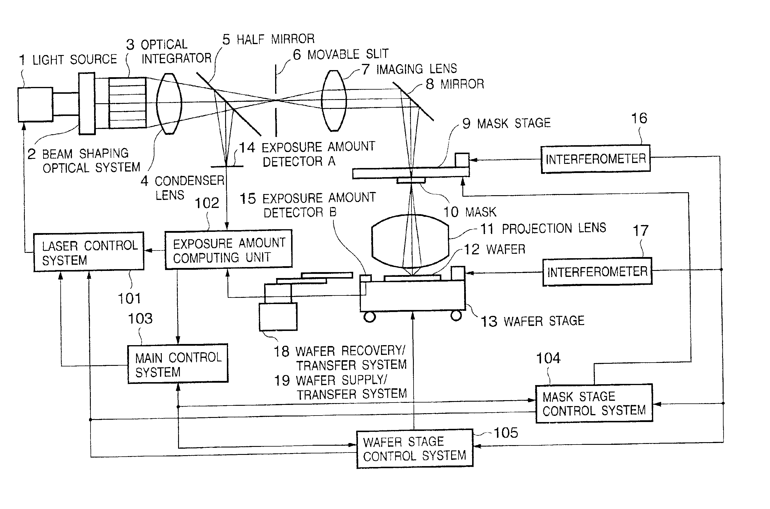
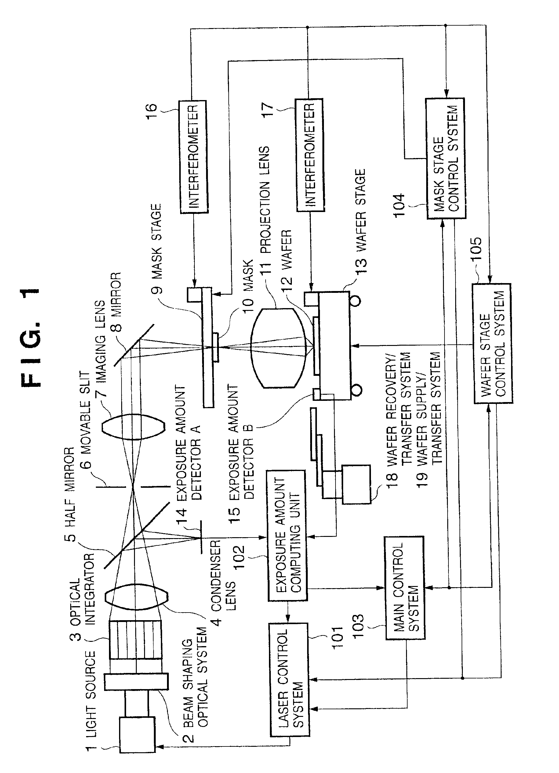
[0050]FIG. 1 is a schematic view showing an exposure apparatus according to an embodiment of the present invention. In this case, a pulse laser such as an excimer laser is used as an exposure light source. A light beam L emitted from a light source 1 formed by a pulse laser such as an excimer laser is shaped into a predetermined shape by a beam shaping optical system 2 and incident on an optical integrator 3. The optical integrator 3 is formed by a flyeye lens constituted by a plurality of microlenses, and has a plurality of secondary sources near its light exit surface. Light beams from the secondary sources near the light exit surface of the optical integrator 3 illuminate, through a condenser lens 4, a movable slit 6 whose aperture shape can be changed. Reference numeral 14 denotes an exposure amount detector A for detecting the amount of part of illumination light split by a half mirror 5 and outputting the resultant signal to an exposure amount computing unit ...

second embodiment

(Second Embodiment)

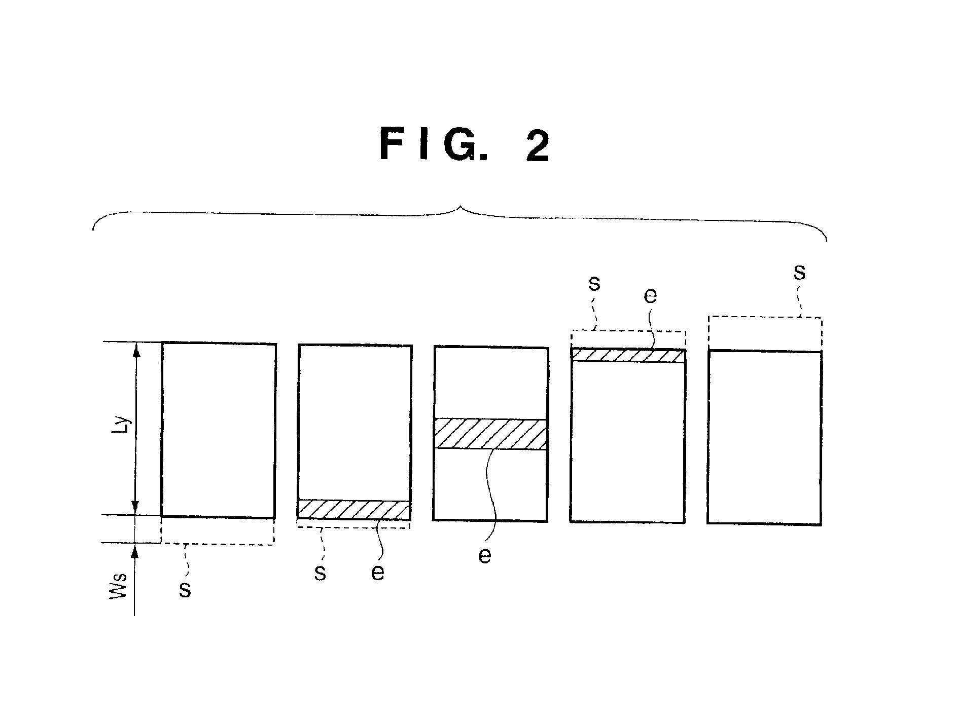
[0107]The second embodiment of the present invention will be described. In this case, FIGS. 3B and 5 show the relationship between the shot layout on a wafer, the wafer stage velocity, and the mask stage velocity.

[0108]When a slit-like light beam moves from a shot area B to a shot area C, the wafer stage starts decelerating at exposure end time t_B3 in FIG. 4. In this case, however, even after the exposure ends at time t_B3, the wafer stage moves at the same velocity as that in the exposure operation, and starts decelerating at time t_B4 to decrease the velocity to 0 at an approach start position for exposure of the shot area C. The wafer stage reaches the approach start position for exposure of the shot area C at time t_B6 (t_C0).

[0109]In this case, a length L that the wafer stage scans at a constant velocity in one scanning operation is expressed by L>Ly+Ws instead of L=Ly+Ws. The length L varies for each shot area, and a scanning velocity Vscan.minB in the shot...


PUM


Abstract

A scanning exposure apparatus includes a master stage for scanning a master, a substrate stage for scanning a substrate, a transfer device for supplying/recovering the substrate to/from the substrate stage, a positioning device for relatively positioning the substrate and the master, and a scanning velocity determination device for determining a scanning velocity so as to maximize the number of substrates that can be exposed per unit time.

Description

FIELD OF THE INVENTION[0001]The present invention relates to an exposure apparatus used in a lithography step of the steps in manufacturing a device, e.g., a semiconductor device such as an IC or LSI, a liquid crystal device, an image sensing device such as a CCD, or a magnetic head, and a device manufacturing method using the exposure apparatus.BACKGROUND OF THE INVENTION[0002]In a manufacturing process of a semiconductor integrated circuit, an exposure apparatus is used to form a pattern on a photosensitive material (to be referred to as a “resist” hereinafter) on a substrate (to be referred to as a “wafer” hereinafter). With an increase in the area of recent semiconductor integrated circuits and an advance in micropatterning, a scanning exposure apparatus called a step-and-scan exposure apparatus designed to illuminate part of a pattern on a mask as a master in the form of a slit, and to perform exposure by synchronously scanning the mask and a wafer at a constant velocity is rep...

Claims


Application Information

Patent Timeline
IPC IPC(8): G03B27/42G03F7/20G03F7/22H01L21/027
CPCG03B27/42G03F7/70725G03F7/70358
Inventor HIURA, MITSURU
Owner OKI ELECTRIC IND CO LTD
Why Eureka
Try Eureka