Method and system of drying materials and method of manufacturing circuit boards using the same

Inactive Publication Date: 2005-05-17
PANASONIC CORP
View PDF12 Cites 33 Cited by
  • Summary
  • Abstract
  • Description
  • Claims
  • Application Information

AI Technical Summary

Benefits of technology

[0014]In order to address the above-mentioned problems, a method of manufacturing circuit boards in accordance with the present invention includes a bonding step of bonding a film-like material to at least one side of a board material to form a substrate material having a film(s). The method of manufacturing circuit boards also includes: a hole-forming step of drilling a through or a blind hole in the board material made of a plurality of materials; and a step of forming a connection means in the through or blind hole for mutually connecting circuits formed on or in the circuit board. The hole-forming step includes: a step of irradiating the board material with laser to form a throug

Problems solved by technology

In the technique of making fine holes and connecting layers using conductive paste, a few foreign substances may cause contact failure.
However, both drilling and laser machining produce a large amount of dust and debris from the cutting process, and this dust and debris may adhere to the board material and close the holes for electrical connection.
In addition, it is also possible that a little dust in air may close the fine holes.
However, because complete cleaning of the holes by a dry cleaning method is very difficult, such new wet cleaning methods as ult

Method used


Image

  • Method and system of drying materials and method of manufacturing circuit boards using the same
  • Method and system of drying materials and method of manufacturing circuit boards using the same
  • Method and system of drying materials and method of manufacturing circuit boards using the same

Examples


Embodiment Construction

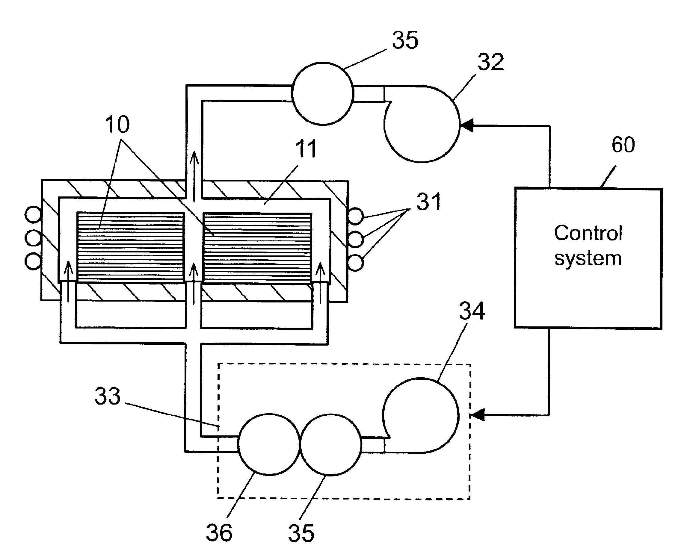
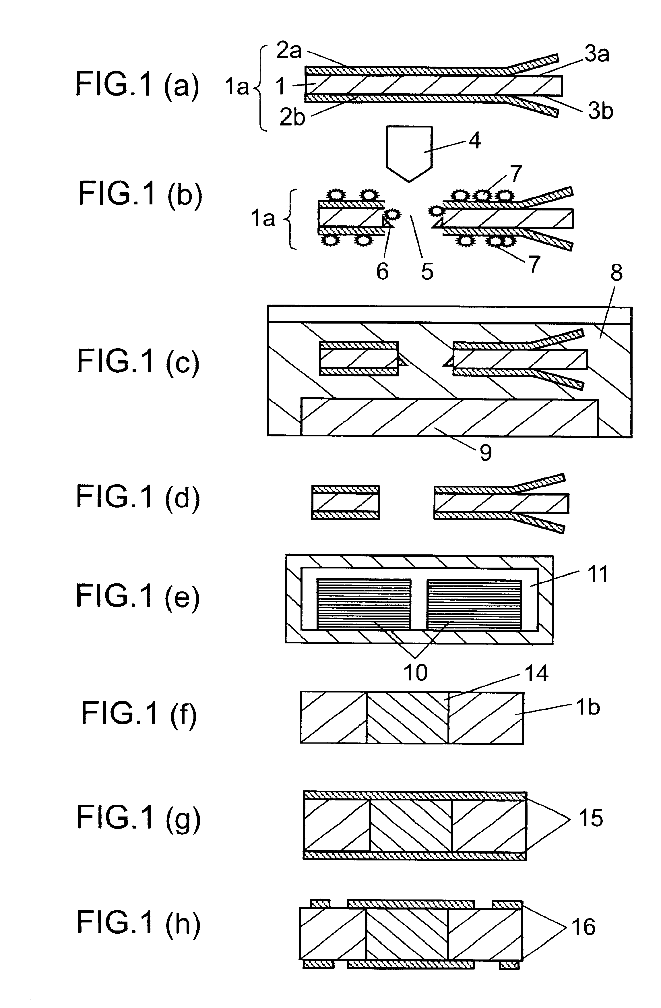
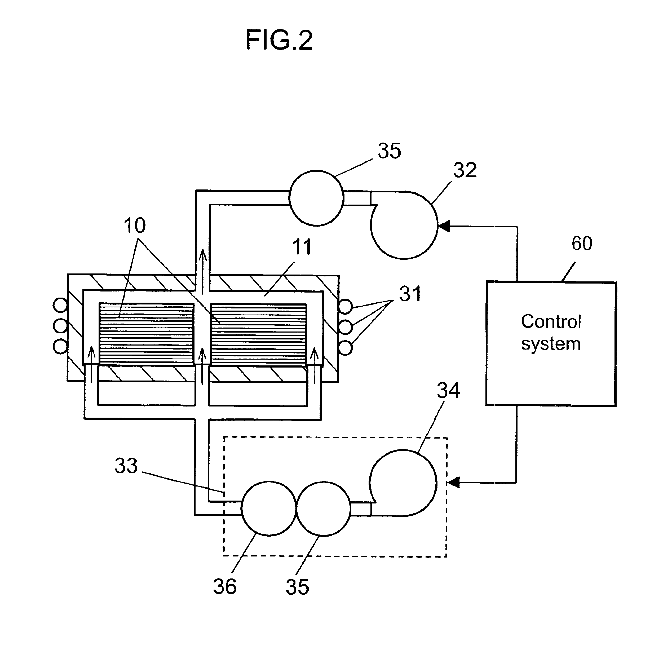
[0020]An exemplary embodiment of the present invention is hereinafter described with reference to FIGS. 1 to 3.

[0021]FIGS. 1(a) to 1(h) show cross sectional views of a process of a method of manufacturing a multi-layered circuit board in accordance with the present embodiment.

[0022]In FIGS. 1(a)-1(h), reference numeral 1 shows a substrate material that is a square plate of 250 mm on each side and approx. 150 μm thick, as an insulating substrate. Used as the substrate material is a resin impregnated substrate made of a composite material in which an non-woven fabric made of an aromatic polyamide fiber (hereinafter referred to as “aramid fiber”) is impregnated with a thermosetting epoxy resin (hereinafter referred to as “epoxy resin”), for example. The epoxy resin in accordance with the present embodiment is a so-called “B stage” epoxy resin that contains an uncured portion.

[0023]Reference numerals 2a and 2b show strippable resin films for masking films, each of which is approx. 20 μm...


PUM

PropertyMeasurementUnit
Temperatureaaaaaaaaaa
Timeaaaaaaaaaa
Pressureaaaaaaaaaa

Abstract

A method and system of cleaning to remove cutting dust and the like generated and adhering to a board material (1a) during drilling for electrical connection, and drying the board material, in a process of manufacturing a circuit board for small electronic equipment and the like. A large amount of board materials can be treated without receiving thermal damage by performing the steps of: placing sheets of the board material that have absorbed moisture resulting from cleaning, like a stack in a vacuum chamber (11); and drying the board material by repeating evacuation and pressurization under predetermined conditions while heating the board material.

Description

[0001]This application claims priority from and is a continuation in part of International Application No. PCT / JP01 / 04819, filed Jun. 7, 2001 and Japanese Patent Application No. 2000-171539, filed Jun. 8, 2000.FIELD OF THE INVENTION[0002]The present invention relates to a method and system of drying materials and a method of manufacturing circuit boards using the same.BACKGROUND OF THE INVENTION[0003]With recent downsizing and high density of electronic equipment, a double-sided or multi-layered circuit board is employed more frequently than a conventional single-sided board, as a circuit board on which electronic components are mounted, and a high density circuit board allowing a larger number of circuits to be integrated in a circuit board is developed.[0004]For the high density circuit board, instead of drilling of holes (through holes) in the board, which is conventionally operated, employment of laser machining capable of faster and more fine machining is developed (Y. Yamanaka...

Claims


Application Information

Patent Timeline
IPC IPC(8): F26B5/04H05K3/40H05K3/22H05K3/00
CPCF26B5/04H05K3/227H05K3/4069H05K3/0032H05K3/0055H05K2203/1461H05K2201/0355H05K2203/0191H05K2203/081H05K2203/085
Inventor KISHIMOTO, KUNIONISHII, TOSHIHIROTAKENAKA, TOSHIAKINAKAMURA, SHINJIMIURA, AKIHIRO
Owner PANASONIC CORP
Why Eureka
Try Eureka