
Single chip ASIC and compact packaging solution for an avalanche photodiode (APD) and bias circuit

a technology of avalanche photodiodes and compact packaging solutions, applied in the field of single chip asic and compact packaging solutions for avalanche photodiodes and its bias and temperature compensation circuits, can solve the problems of increasing the complexity of the package itself and the mechanical design of the board on which it is mounted, and causing the avalanche to be driven further into

Active Publication Date: 2005-05-17
OPLINK COMM
View PDF5 Cites 54 Cited by
  • Summary
  • Abstract
  • Description
  • Claims
  • Application Information

AI Technical Summary

Benefits of technology

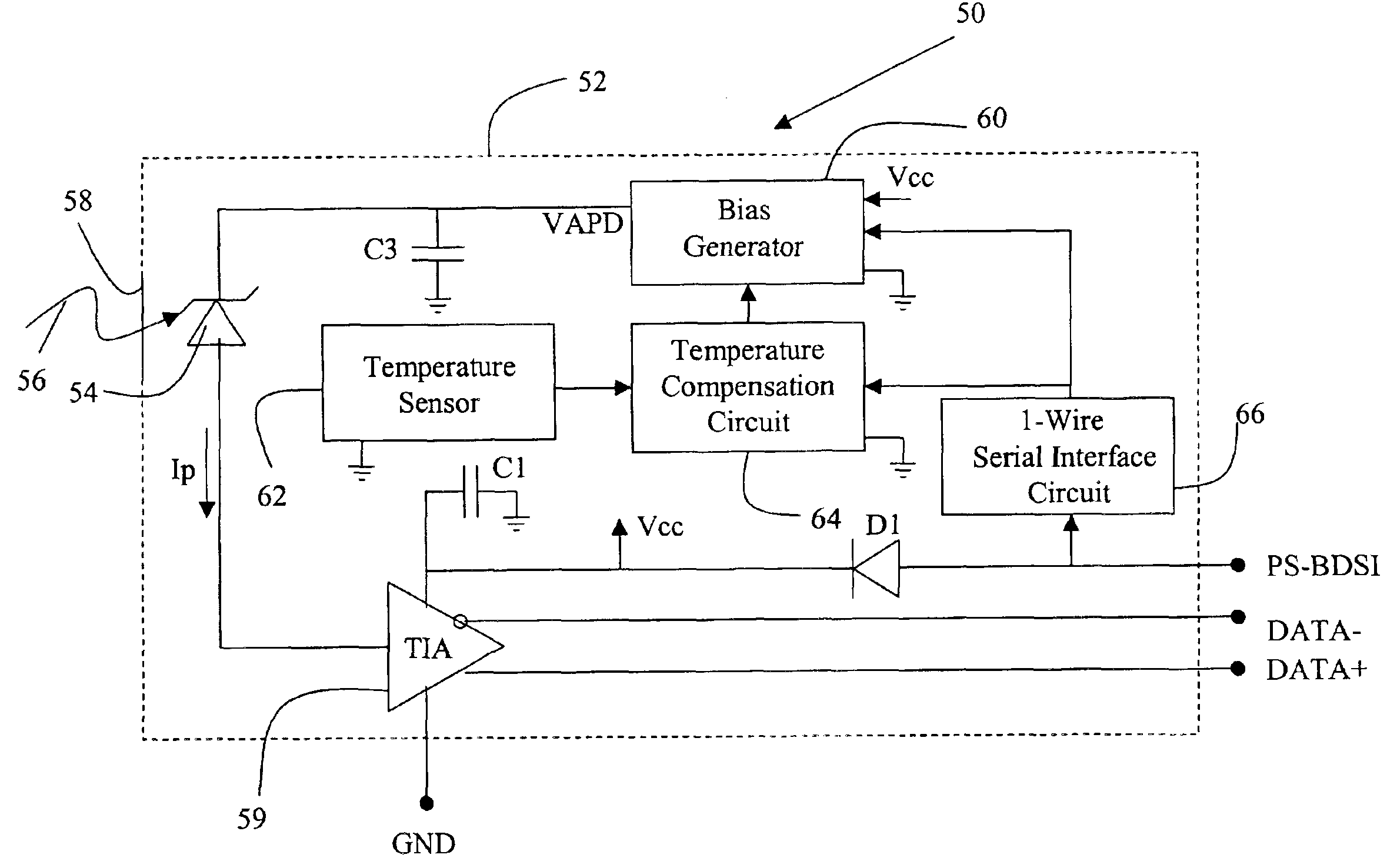
[0014]The present invention provides a compact integrated APD package that integrates the bias voltage and temperature compensation functions inside a standard 4-pin PIN diode package such as the TO-46 can with fewer parts. The APD package is substantially plug and play compatible with existing applications designed for PIN diodes with slight modifications for communication of control information to and from the integrated APD package to an external controller circuit.
[0015]This is accomplished by integrating the active components of the bias and temperature compensation circuits into a single ASIC using a high-voltage CMOS process and operating at frequencies of at least 1 MHz to reduce the size of the passive components. The combination of single-chip ASIC integration and smaller passives allows this circuitry to be packaged inside a standard 4-pin TO-46 package. To mount the relatively large ASIC chip inside the package with the APD chip, TIA chip and passives the 4-pin package may be modified by either recessing the pins inside the can to facilitate surface mounting the ASIC or adding a spacer or submount inside the can to facilitate three-dimensional packaging. Communication with the bias and temperature circuits is accomplished using a unique 1-wire serial interface circuit via the power supply pin. A clock signal is preferably embedded in the control data to synchronize the APD with an external controller. Communication is preferably bi-directional but serial-in may be applicable in some cases.

Problems solved by technology

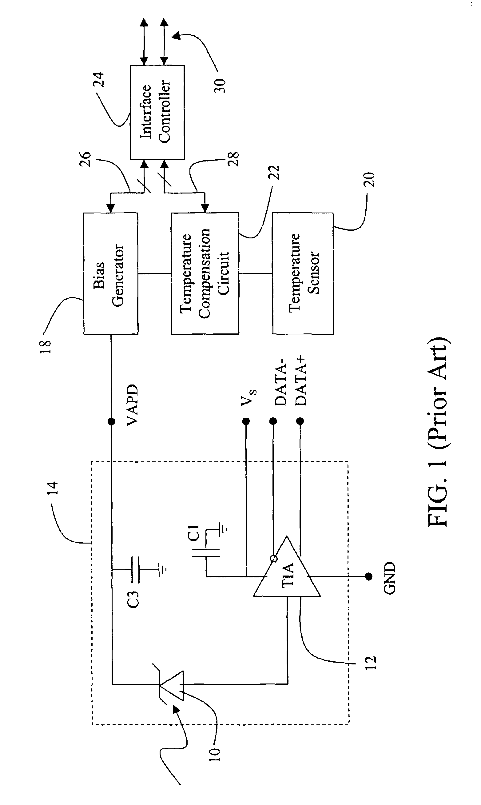
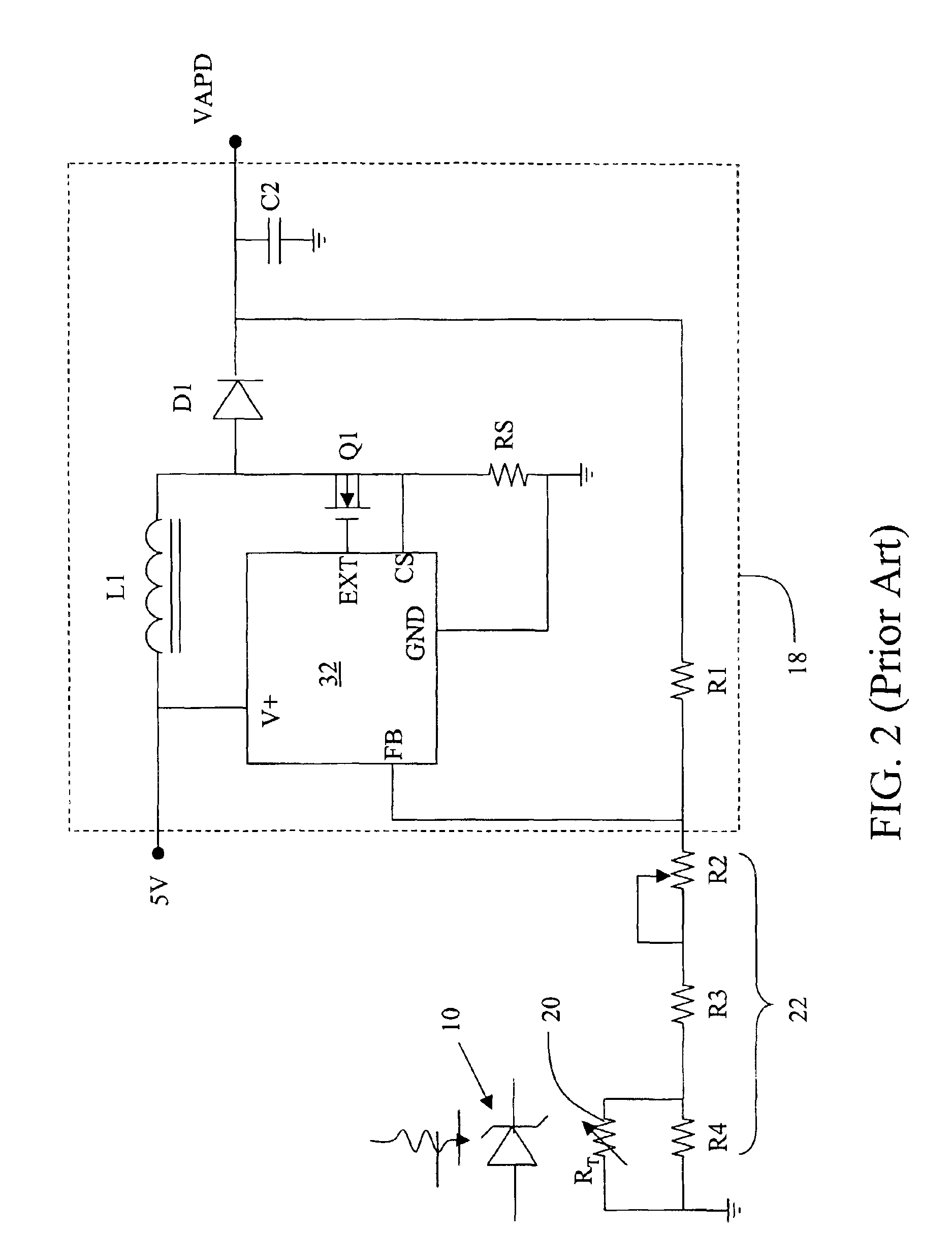
This enhancement of sensitivity, however, is achieved at the expense of having to provide a high voltage bias circuit that accurately controls a bias voltage (VAPD) of the APD, which is complicated by the fact that the APD gain and therefore the reverse bias requirement is temperature dependent.
Failure to do so can cause the APD to be driven further into breakdown where it becomes exceedingly noisy, thereby drastically reducing the signal to noise ratio of the system.
The addition of the fifth pin increases the complexity of the package itself and the mechanical design of the board on which it is mounted.
As a result, the passive components (inductors and capacitors) are large.
The lack of integration into a single IC chip and the size of the passive components necessitate placement of the bias generator outside the APD package and provisioning of the bias voltage via the fifth pin.
However, the external bias and temperature circuits occupy valuable space on the optical transceiver PC board, for example, and increase parts count, hence cost.
The fifth pin also complicates the packaging of the device.
The current multi-chip ASIC solution cannot scale down in either size or cost to meet this demand.

Method used


Image

  • Single chip ASIC and compact packaging solution for an avalanche photodiode (APD) and bias circuit
  • Single chip ASIC and compact packaging solution for an avalanche photodiode (APD) and bias circuit
  • Single chip ASIC and compact packaging solution for an avalanche photodiode (APD) and bias circuit

Examples


Embodiment Construction

[0031]The present invention provides an APD package that integrates the bias voltage and temperature compensation functions inside a standard 4-pin Detector / TIA hybrid TO-46 package. The APD package is substantially plug and play compatible with existing applications designed for PIN / TIA hybrid packages with slight modifications for communications of control information to and from the integrated APD package to a controller circuit. All of the active components of the bias and temperature compensation circuits are integrated into a single ASIC using a high-voltage CMOS process, capable of operating up to at least 70V, which is operated at frequencies of at least 1 MHz to greatly reduce the size of the passive components. The combination of single-chip ASIC integration and much smaller passive components allows this circuitry to be packaged inside a standard 4-pin package. Small internal modifications to the package in the form of recessed pins or a spacer / submount may be needed to f...


PUM


Abstract

A compact integrated APD device integrates the bias voltage and temperature compensation functions inside a standard 4-pin PIN package. The active components of the bias and temperature compensation circuits are integrated into a single ASIC using a high-voltage CMOS process and operated at frequencies of at least 1 MHz to greatly reduce the size of the passive components. To mount the relatively large ASIC chip inside the package with the APD chip, TIA chip and passives, the 4-pin package may be modified by either recessing the pins inside the can to facilitate surface mounting the ASIC or adding a spacer inside the can to facilitate three-dimensional packaging. Communication with the bias and temperature circuits is accomplished using a unique bi-directional 1-wire serial interface via the power supply pin. A clock signal is preferably embedded in the control data to synchronize the APD with an external controller.

Description

BACKGROUND OF THE INVENTION[0001]1. Field of the Invention[0002]This invention relates to avalanche photodiodes (APD's) used in optical communication systems and more specifically to a single chip ASIC and compact packaging solution for an APD and its bias and temperature compensation circuits.[0003]2. Description of the Related Art[0004]PIN photodiodes and avalanche photodiodes (APDs) are both used as detectors in fiber optics communications systems. Standard PIN photodiodes combined with a TransImpedance Amplifier (TIA) to boost the low level signal from the PIN diode are available in compact packages and can be fully interfaced via 4 I / O pins; power supply, ground and a differential output. An industry standard package is the 4-pin TO-46 package or “can”, which is compact, BellCor qualified and designed into many optical applications. The 4-pin TO-46 can has differential output pins DATA and DATA−, power supply pin Vs and ground pin GND. The term “pin” as used herein is intended ...

Claims


Application Information

Patent Timeline
IPC IPC(8): H01J40/00H01J40/14
CPCH03K19/14H03K19/00369
Inventor RICHARD, JENKIN ANGELOGILLILAND, PATRICK B.CHAMNESS, ERIC VAUGHANANGUELOV, EVGUENIY DIMITROV
Owner OPLINK COMM
Learn More