Thin film capacitor having multi-layer dielectric film including silicon dioxide and tantalum pentoxide

a thin film capacitor and dielectric film technology, applied in the direction of semiconductor/solid-state device details, transistors, solid-state devices, etc., can solve the problems of oxygen deficiency defects, too large increase, and increase the current of leakage, so as to reduce the roughness of the first layer, prevent current leakage, and reduce the effect of roughness

Inactive Publication Date: 2005-05-17
TECH IP HLDG
View PDF5 Cites 5 Cited by
  • Summary
  • Abstract
  • Description
  • Claims
  • Application Information

AI Technical Summary

Benefits of technology

[0009]A capacitor and a method of forming the same is disclosed, one embodiment of which includes depositing a multi-layer dielectric film between first and second spaced-apart electrodes. The multi-layer dielectric film includes first and second layers that have differing roughness. The layer of the dielectric film having the least amount of roughness is disposed adjacent to the first electrode. After depositing the second layer of the dielectric film adjacent to the first layer, the second layer is annealed. It is believed that the reduced roughness of the first layer reduces pin-hole formation in the second layer. In this manner, current leakage is prevented, or reduced, in the resulting thin-film capacitor, while providing suitable capacitance and breakdown voltage. An exemplary embodiment of the thin-film capacitor forms the dielectric material from silicon dioxide (SiO2)and tantalum pentoxide (Ta2O5). To provide the thin-film capacitor with the desired operational characteristics, the layer of tantalum pentoxide is provided with a thickness that is approximately three times greater than the thickness of the silicon dioxide layer. To that end, in the exemplary method, the first electrode is formed by vapor deposition of phosphorous oxytrichloride (POCl3). The layer of silicon dioxide is formed by thermal oxidation of silicon in oxygen. The layer of tantalum pentoxide is formed by sputtering tantalum (Ta) onto the layer of silicon dioxide in an oxygen rich ambient. Annealing then densities the tantalum oxide. Thereafter, the second electrode is formed by deposition of a layer consisting of aluminum, chromium, copper, titanium, titanium nitride, titungsten or a combination thereof.

Problems solved by technology

Although increasing the film thickness may reduce the leakage current and increase the capacitance, too great an increase exacerbates leakage current due to the increased stress it places on the tantalum pentoxide film.
These are believed to be caused by diffusion of electrode metal atoms into the dielectric and diffusion of oxygen out, creating oxygen deficiency defects.

Method used


Image

  • Thin film capacitor having multi-layer dielectric film including silicon dioxide and tantalum pentoxide
  • Thin film capacitor having multi-layer dielectric film including silicon dioxide and tantalum pentoxide
  • Thin film capacitor having multi-layer dielectric film including silicon dioxide and tantalum pentoxide

Examples


Embodiment Construction

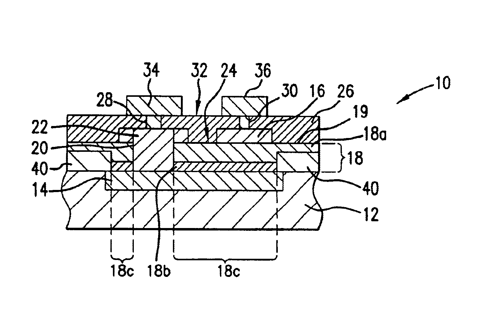
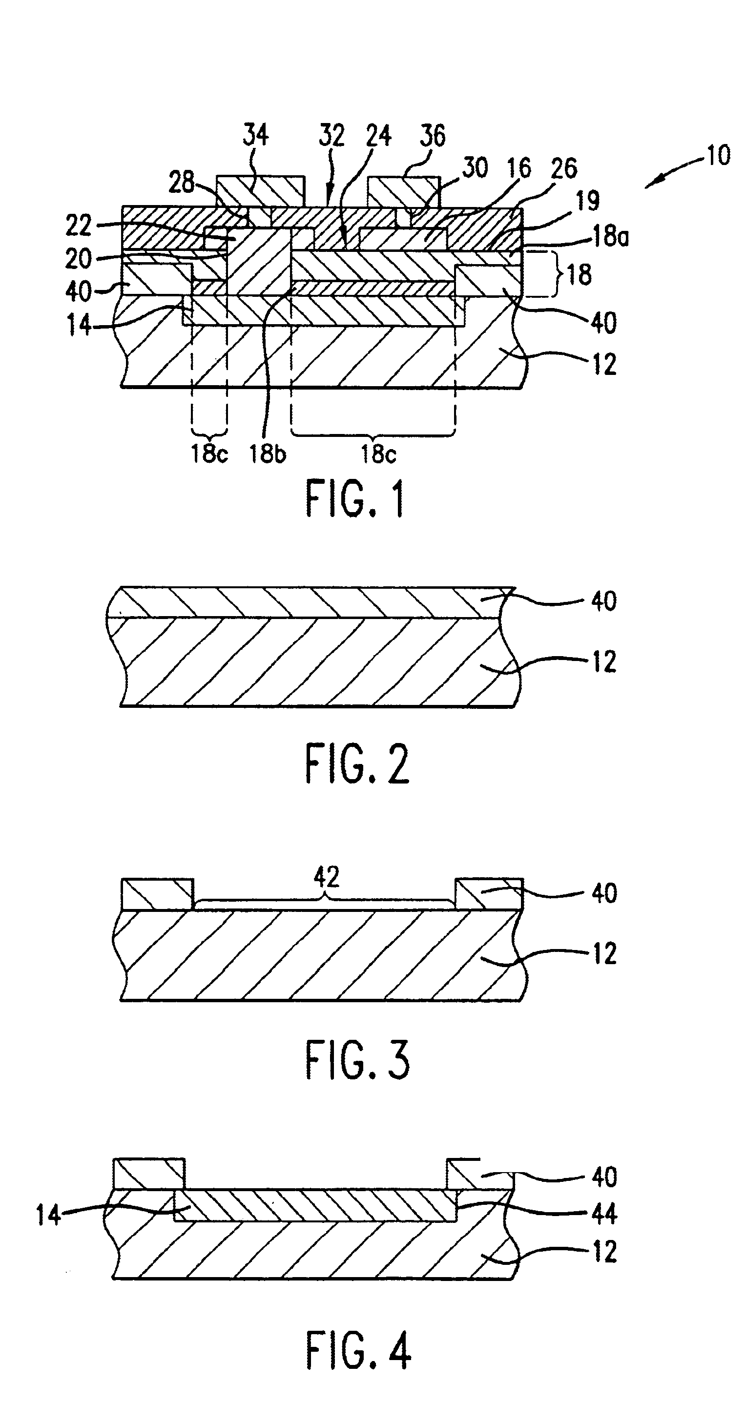
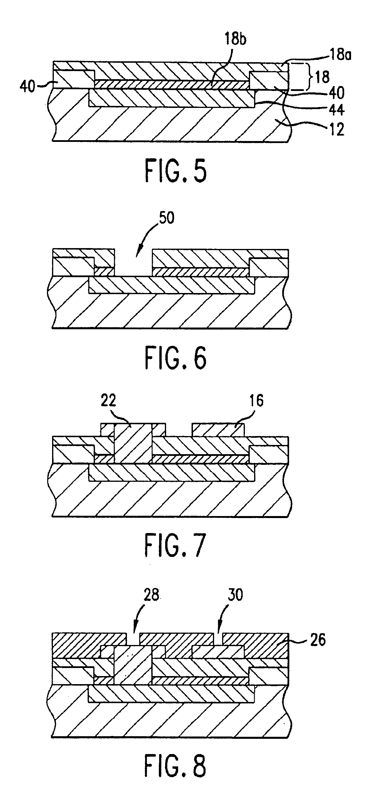
[0019]FIG. 1 is a cross-sectional view of an exemplary thin-film capacitor 10 in accordance with the present invention that is formed atop of a substrate 12. Capacitor 10 includes a pair of spaced-apart electrodes 14 and 16, with a multi-layer dielectric film 18 disposed therebetween. A via 20 is formed through dielectric film 18 and extends from a surface 19 thereof, terminating proximate to electrode 14. A conductive contact 22 is formed in via 20 so as to extend from electrode 14 away from surface 24 of dielectric material 18. Contact 22 is formed adjacent to, but spaced-apart from, electrode 16. Formed adjacent to the capacitive structure is a dielectric layer that is typically formed from a layer of Benzocyclobutene (BCB), shown as BCB layer 26. First and second throughways 28 and 30 are formed in BCB layer 26. First throughway 28 extends from an upper surface 32 of BCB layer 26, terminating proximate to the contact 22, and second throughway 30 extends from upper surface 32, te...


PUM

PropertyMeasurementUnit
thickaaaaaaaaaa
thickaaaaaaaaaa
breakdown voltageaaaaaaaaaa

Abstract

A capacitor and a method of forming the same, one embodiment of which includes depositing a multi-layer dielectric film between first and second spaced-apart electrodes. The multi-layer dielectric film includes first and second layers that have differing roughness. The layer of the dielectric film having the least amount of roughness is disposed adjacent to the first electrode. After depositing the second layer of the dielectric film adjacent to the first layer, the second layer is annealed. An exemplary embodiment of the thin film capacitor forms the dielectric material from silicon dioxide (SiO2) and tantalum pentoxide (Ta2O5).

Description

CROSS-REFERENCE TO RELATED APPLICATION[0001]This application is a divisional of U.S. patent application Ser. No. 10 / 093,961 filed on Mar. 8, 2002 now U.S. Pat. No. 6,620,673 entitled “THIN FILM CAPACITOR HAVING MULTI-LAYER DIELECTRIC FILM INCLUDING SILICON DIOXIDE AND TANTALUM PENTOXIDE,” which is incorporated herein by reference in its entirety.FIELD OF THE INVENTION[0002]The present invention relates to a method for manufacturing a semiconductor thin film capacitor. More particularly, the present invention is directed to a method for manufacturing a thin film capacitor having a dielectric film formed of tantalum oxide.BACKGROUND OF THE INVENTION[0003]The operational characteristics of thin film capacitors become increasingly important as the operation frequency of the various circuits in which these capacitors are included increases. Examples of such circuits include dynamic random access memories, in which the thin-film capacitor is employed as a storage cell; filters, in which t...

Claims


Application Information

Patent Timeline
Patent Type & Authority Patents(United States)
IPC IPC(8): H01L21/02H01L21/316
CPCH01L28/40H01L21/31612H01L28/56H01L21/31637H01L21/02266H01L21/02238H01L21/02164H01L21/02183H01L21/02255H01L21/022
Inventor LAFLEUR, MIKE
Owner TECH IP HLDG
Why Eureka
Try Eureka