Transparent conductive film and touch panel

a technology of transparent conductive film and touch panel, which is applied in the direction of instruments, natural mineral layered products, transportation and packaging, etc., can solve the problems of spoiling electrical properties, low productivity and high production cost, and limited heat treatment temperature, and achieve good reliability and durability.

Inactive Publication Date: 2005-05-24
BRIDGESTONE CORP
View PDF10 Cites 38 Cited by
  • Summary
  • Abstract
  • Description
  • Claims
  • Application Information

AI Technical Summary

Benefits of technology

[0007]It is an object of the present invention to solve the aforementioned conventional problems, to provide a transparent conductive film comprising a polymer film and a transparent conductive layer formed on the polymer film, which can realize a touch panel having no problem of damage and delamination of the transparent conductive layer, and having good reliability and durability, and to provide a touch panel provided with the transparent conductive film.

Problems solved by technology

However, since the substrate of the transparent conductive film is a polymer film, the temperature for the heat treatment is limited.
This causes problems of low productivity and high production cost.
When the transparent conductive layer 5 of the upper electrode 6 is damaged or delaminated, electrical resistivity of the surface of the transparent conductive layer 5 changes, and uniformity of the electrical resistivity is lost, thereby spoiling electrical properties, and thus the precise input can not be carried out.
These cause a decrease in reliability of the touch panel, damages, defects, and a decrease in durability.

Method used


Image

  • Transparent conductive film and touch panel
  • Transparent conductive film and touch panel
  • Transparent conductive film and touch panel

Examples


example 1

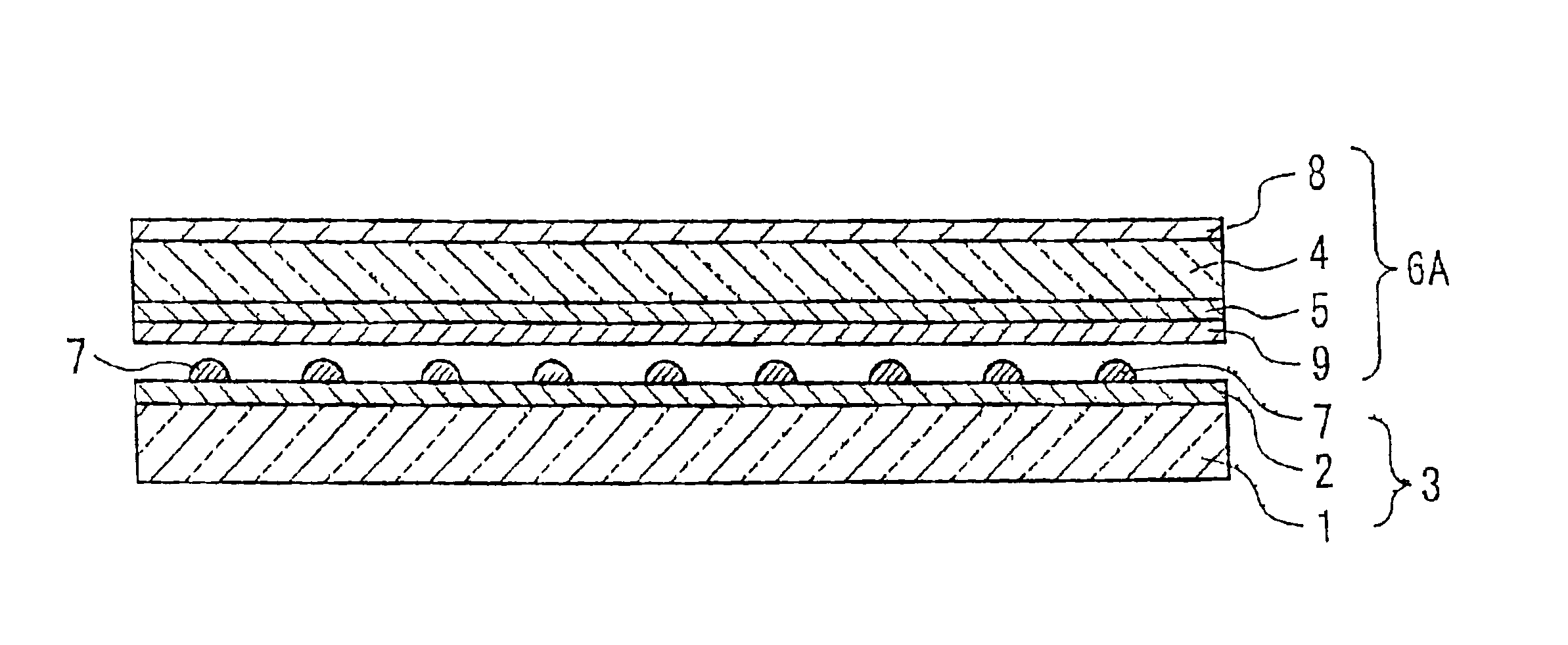
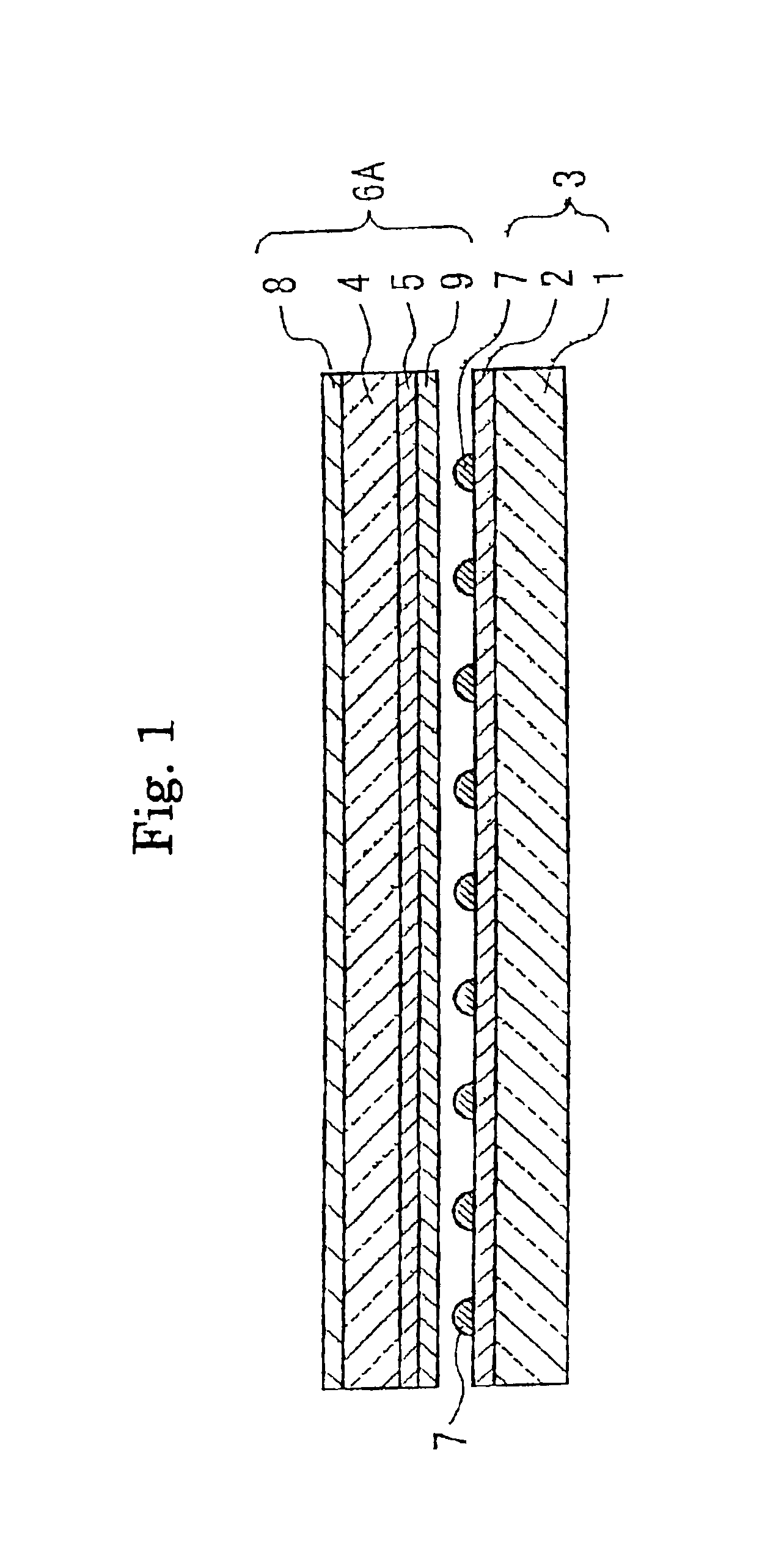
[0075]A PET film having a thickness of 188 μm was employed as a substrate. A hard-coating layer with a thickness of 5 μm was, firstly, formed on one surface of the PET film by wet coating an acryl-based UV-curing hard coating material (Z7501 manufactured by JSR corporation, in which the solid content was 35% by weight and the solvent thereof was methyl ethyl ketone.).

[0076]The film was set in a magnetron RF sputtering device with both a sintered ZnO—Al target including 2% by weight of Al2O3 and having a purity of 99.99% and a graphite target having a purity of 99% as targets of a transparent conductive layer.

[0077]The sputtering device was evacuated with a turbo-molecular pump to lower its internal pressure to 1×10⁻⁴ Pa, and then Ar gas was introduced into the sputtering device at flow rate of 200 sccm to hold the internal pressure at 0.3 Pa. After that, the sintered ZnO—Al target was applied with RF voltage, so that an Al-doped ZnO thin layer having a thickness of about 80 nm was d...

example 2

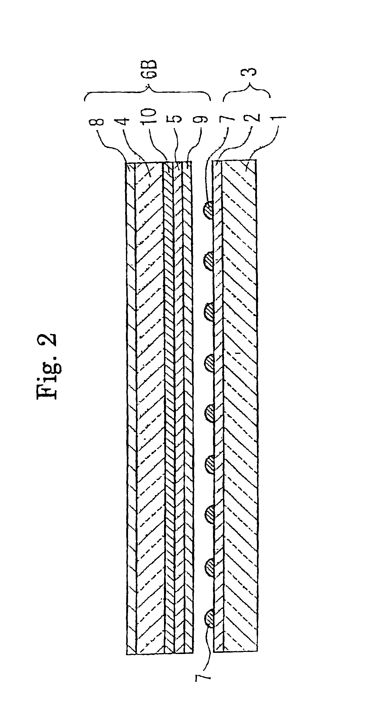
[0081]A transparent conductive film was produced in the same manner as in Example 1 except that an SiC target was used instead of the graphite target and an SiC thin layer having a thickness of about 3 nm was deposited as a covering layer.

[0082]The resulted transparent conductive film was measured in the surface resistivity and the resistance to sliding wear in the same manner as in Example 1. The results are shown in Table 1.

[0083]The SiC target used in Example 2 was obtained by mixing SiC powder with 20% by weight of phenolic resin as a sintering assistant uniformly and sintering at 2100° C. The SiC target had a density of 2.92 g / cm3.

example 3

[0084]A transparent conductive film was prepared in the same manner as in Example 2 except that after the Al-doped ZnO transparent conductive layer was deposited, mixed gas of 170 sccm Ar gas and 30 sccm O2 gas was introduced into the chamber to hold the internal pressure at 0.5 Pa, and then the SiC target was applied with DC pulse voltage, so that an SiCxOy (x=0.05, y=1.9) thin layer having a thickness of about 3 nm was deposited as a covering layer.

[0085]The resulted transparent conductive film was measured in the surface resistivity and the resistance to sliding wear in the same manner as in Example 1. The results are shown in Table 1.


PUM

PropertyMeasurementUnit
thicknessaaaaaaaaaa
densityaaaaaaaaaa
temperatureaaaaaaaaaa

Abstract

A transparent conductive film has a polymer film 4 and a transparent conductive layer 5 formed on the polymer film 4. The transparent conductive layer includes indium oxide, a zinc oxide system and a tin oxide system. A covering layer 9, made of material different from that of the transparent conductive layer 5, is formed on the transparent conductive layer 5. A touch panel is provided with the transparent conductive film as its upper electrode 6A or lower electrode. The surface of the transparent conductive layer is covered with the covering layer, so that physical or chemical stresses generated during the input to the touch panel do not affect transparent conductive layer directly, thus preventing damages and delamination of the transparent conductive layer. Furthermore, the covering layer formed on the transparent conductive layer improves the strength of the transparent conductive film, thereby enhancing a resistance to wear.

Description

FIELD OF THE INVENTION[0001]The present invention relates to a transparent conductive film having a polymer film and a transparent conductive layer formed on the polymer film, wherein the conductive layer is resistant fully to delamination or removal and the conductive film has good electrical characteristics and good durability. The present invention further relates to a touch panel provided with the transparent conductive film.BACKGROUND OF THE INVENTION[0002]A resistive touch panel is widely used as an input unit for a household appliance or a portable terminal because the touch panel is easy to be miniaturized, lightened, and thinned. When a user pushes a part of the touch panel or draws with a specialized pen on a part of the touch panel, the part comes into contact with an opposing electrode, so that the portion and the electrode are electrically connected and a signal is inputted.[0003]As shown in FIG. 4, a typical resistive touch panel has a lower electrode 3 having a glass ...

Claims


Application Information

Patent Timeline
Patent Type & Authority Patents(United States)
IPC IPC(8): B32B15/04B32B9/00C03C27/06C03C27/08
CPCG06F3/045G06F2203/04103Y10T428/12618Y10T428/2949Y10T428/30Y10T428/265
Inventor IWABUCHI, YOSHINORIKOBAYASHI, TAICHIOHNO, SHINGOKUSANO, YUKIHIROYOSHIKAWA, MASATO
Owner BRIDGESTONE CORP
Why Eureka
Try Eureka