Capacitor and manufacturing method thereof, semiconductor device and substrate for a semiconductor device

a manufacturing method and semiconductor technology, applied in the direction of printed capacitor incorporation, fixed capacitor details, semiconductor/solid-state device details, etc., can solve the problems of complex process, reduced overall thickness of the substrate, and inability to supply stable electric power to semiconductor chips, etc., to achieve the effect of reducing the distance between the terminal provided on the chip-mounting surface and the capacitor, and reducing the overall thickness of the substra

Active Publication Date: 2005-05-24
SHINKO ELECTRIC IND CO LTD
View PDF3 Cites 39 Cited by
  • Summary
  • Abstract
  • Description
  • Claims
  • Application Information

AI Technical Summary

Benefits of technology

[0035]According to the present invention, the capacitor can be formed with reduced thickness as a result of use of the support body of organic polysilane film, and the overall thickness of the substrate can be reduced as well.
[0036]Because the capacitor is disposed right underneath the chip-mounting surface, the distance between the terminal provided on the chip-mounting surface and the capacitor is minimized, and the inductance associated with a conductor

Problems solved by technology

With sharp increase of clock frequency in recent advanced semiconductor devices, supply of a stable electric power to semiconductor chip is becoming a paramount problem.
Further, there is a need of complex process such as dry etching, wet etching or laser processing at the time of forming a through hole in the silicon substrate 15.
Thus, such a complex process causes further degradation in the efficiency of manufacturing a semiconductor device.
Further, associated with the use of the silicon substrate 15 for the support of the capacitor, there arises a problem that the capacitor 14, and hence the substrate 11, inevitably has a considerable thickness.
Further, bec

Method used


Image

  • Capacitor and manufacturing method thereof, semiconductor device and substrate for a semiconductor device
  • Capacitor and manufacturing method thereof, semiconductor device and substrate for a semiconductor device
  • Capacitor and manufacturing method thereof, semiconductor device and substrate for a semiconductor device

Examples


first embodiment

[First Embodiment]

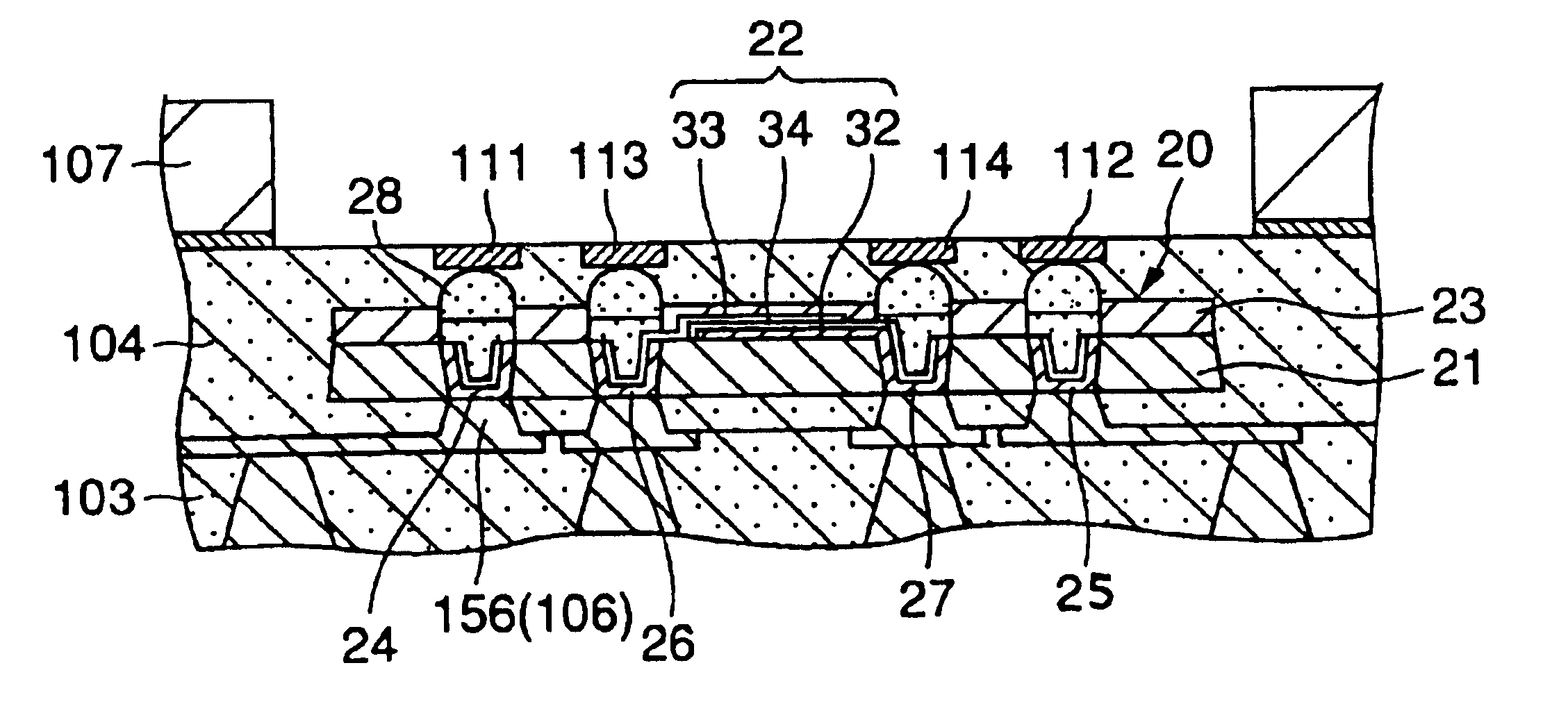
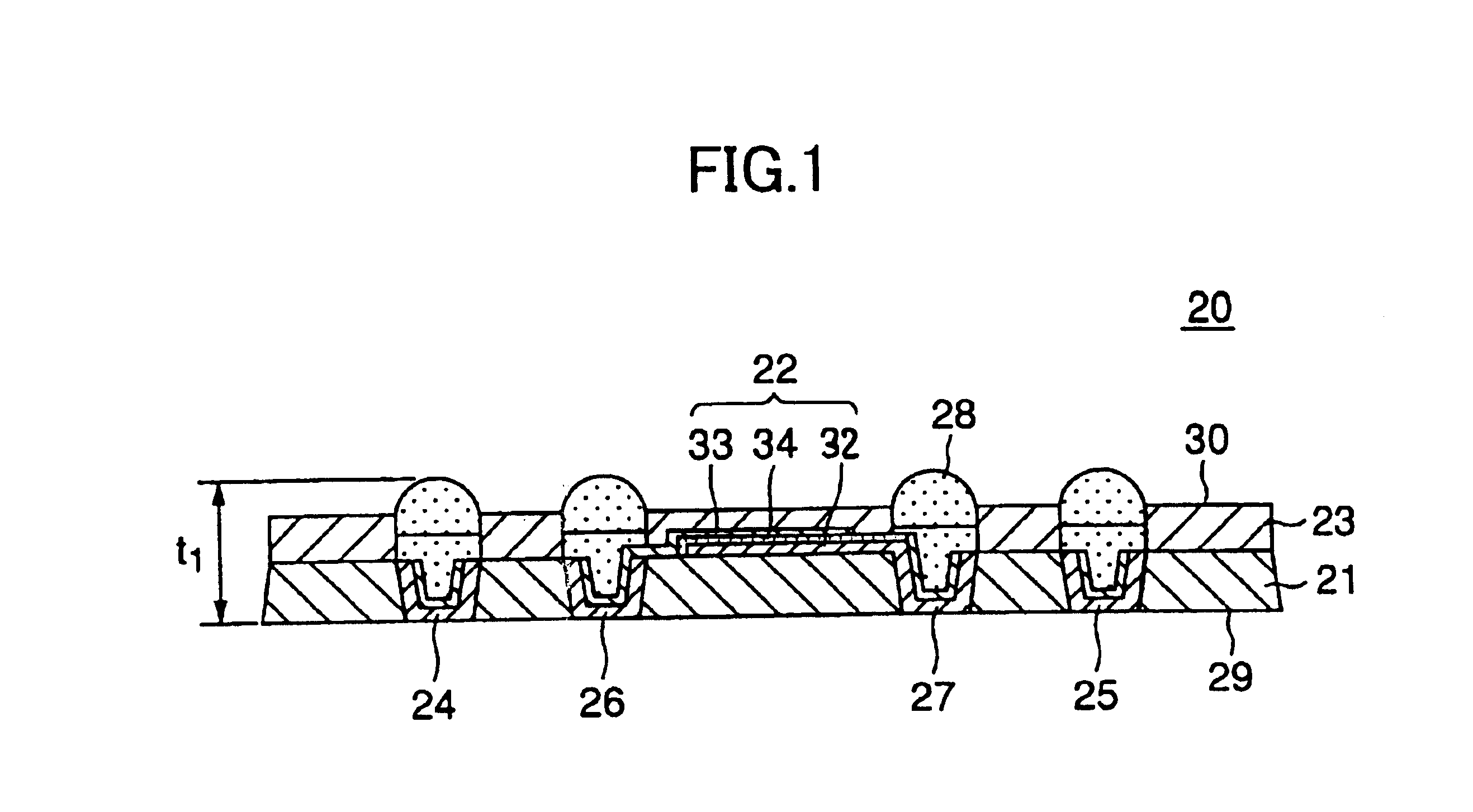
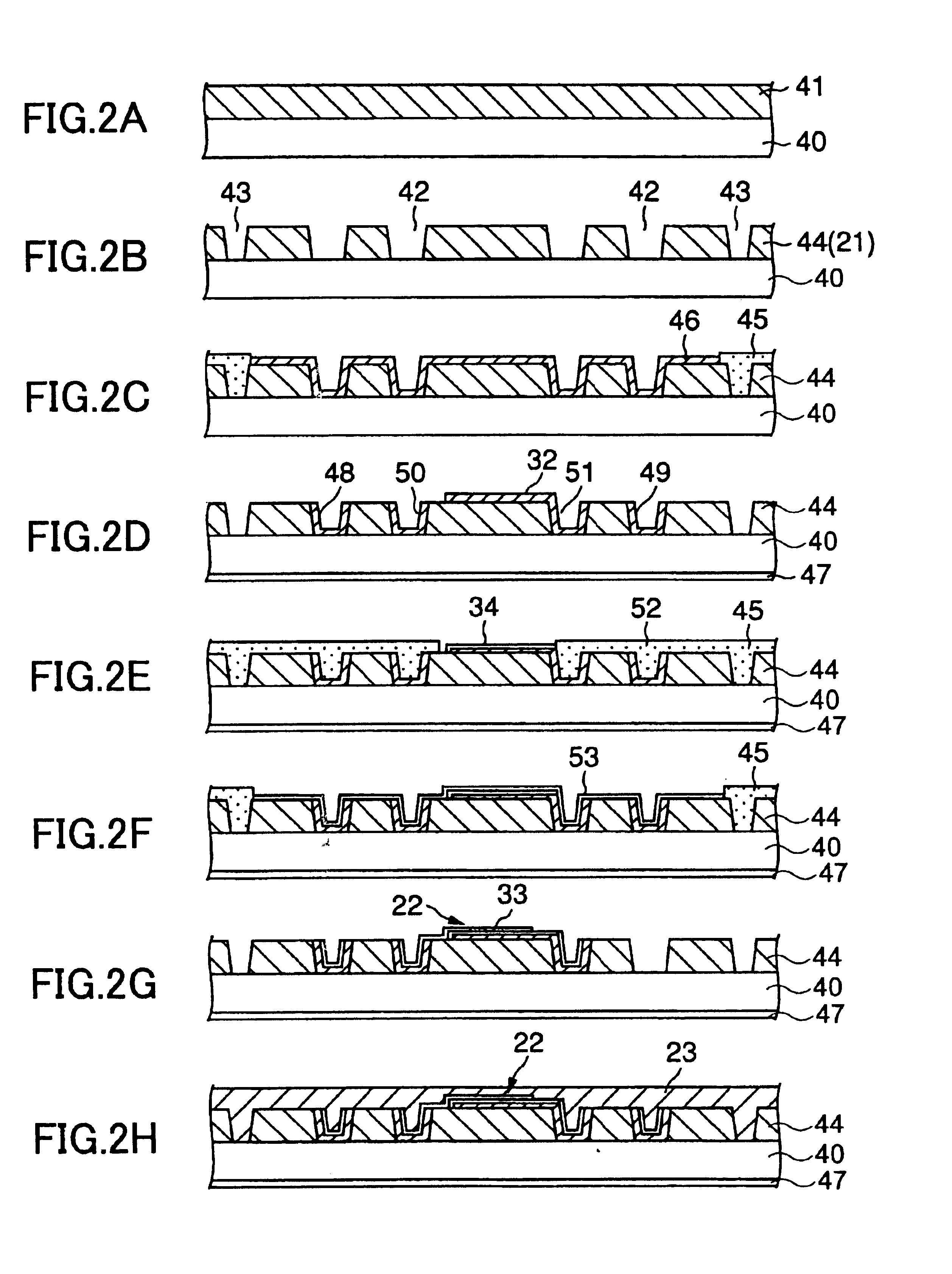
[0078]FIG. 1 shows the construction of a capacitor 20 according to a first embodiment of the present invention.

[0079]Referring to FIG. 1, the capacitor 20 is embedded in a substrate used for carrying a semiconductor chip in the state that the capacitor is exposed at the surface of the substrate, wherein the capacitor constitutes the mounting part of the semiconductor chip. The same holds true in capacitors 20A-20D to be explained later.

[0080]It should be noted that the capacitor 20 has a support body 21 formed of an organic polysilane film. The capacitor 20 has a size similar to that of the semiconductor chip mounted thereon, and includes, in addition to the support body 21, a capacitor part 22 formed on the support body 21 and an insulation layer 23 formed on the support body 21 so as to cover the capacitor part 22, wherein signal electrodes 24 and 25, a power terminal 26 and a ground terminal 27 are exposed at the bottom surface of the support body 21. Further, t...

second embodiment

[Second Embodiment]

[0117]FIG. 4 shows the construction of a capacitor 20A according to a second embodiment of the present invention, wherein the capacitor 20A has a construction similar to that of the capacitor 20 except for the capacitor part and the terminals. Thus, those parts of FIG. 4 corresponding to the parts of FIG. 1 are designated by the same reference numerals and the description thereof will be omitted.

[0118]Referring to FIG. 4, the capacitor 20A has a size similar to the size of the semiconductor chip and includes a capacitor part 22A formed on the top surface of the support body 21 formed of the organic polysilane film. The capacitor part 22A is covered by the insulation film 23 formed on the support body 21, and signal terminals 24A and 25A, a power terminal 26A and a ground terminals 27A are exposed at the bottom surface of the support body 21. Further, solder bumps 28 are provided so as to project from the insulation layer 23.

[0119]The capacitor part 22A of the pres...

third embodiment

[Third Embodiment]

[0138]FIG. 7C shows the construction of a capacitor 20B according to a third embodiment of the present invention.

[0139]Referring to FIG. 7C, the capacitor 20B has a structure similar to that of the capacitor 20A of FIG. 4 except that the solder bumps 28 are not provided. In FIGS. 7A-7C, those parts corresponding to the parts described previously are designated by the same reference numerals and the description thereof will be omitted.

[0140]The capacitor 20B has a size identical with the size of the semiconductor chip and includes a support body 21 of organic polysilane film and a capacitor part 22A formed on the support body 21. Further, the insulation layer 23 covers the capacitor part 22A on the support body 21 and the signal thermals 24A, 25A, power terminal 26A and the ground terminal 27A are exposed at the bottom surface of the support body 21. The insulation layer 23 is formed with the opening 54 such that the opening 54 exposes the pad 65 at the bottom there...


PUM

PropertyMeasurementUnit
Dielectric polarization enthalpyaaaaaaaaaa

Abstract

A capacitor includes a capacitor part formed of a dielectric film sandwiched by a pair of electrodes and a support body formed of a film of an organic polysilane. The support body is provided so as to support the capacitor part thereon.

Description

CROSS-REFERENCE TO RELATED APPLICATION[0001]The present application is based on Japanese priority application No. 2002-314694 filed on Oct. 29, 2002, the entire contents of which are hereby incorporated by reference.BACKGROUND OF THE INVENTION[0002]The present invention generally relates to semiconductor devices and more particularly to a capacitor and manufacturing method thereof as well as a substrate having a capacitor.[0003]With sharp increase of clock frequency in recent advanced semiconductor devices, supply of a stable electric power to semiconductor chip is becoming a paramount problem. In order to deal with this problem, there is a proposal to provide a capacitor on a substrate on which the semiconductor chip is mounted.[0004]FIG. 20 shows a conventional semiconductor device 10.[0005]Referring to FIG. 20, the semiconductor device 10 includes a substrate 11 mounted with a semiconductor chip 12, wherein the substrate 11 includes a substrate body 13 and a decoupling capacitor ...

Claims


Application Information

Patent Timeline
IPC IPC(8): H05K1/16H01L23/12H01G4/224H01L21/68H01L23/50H01L23/64
CPCH01G4/224H01L23/50H01L23/642H05K1/162H01L21/6835H01L2224/16235H01L2221/68345H01L2221/68363H01L2224/16H01L2924/01078H01L2924/01079H01L2924/12044H01L2924/15174H01L2924/15311H01L2924/19041H05K2201/0162H05K2201/09763H01L2924/01019H01L24/05H01L2224/05001H01L2224/05026H01L2224/05172H01L2224/05184H01L2224/05571H01L2224/056H01L2924/00014H01L2224/05147H01L2224/05166
Inventor OOI, KIYOSHIHORIKAWA, YASUYOSHIYAMASAKI, TOMOO
Owner SHINKO ELECTRIC IND CO LTD
Why Eureka
Try Eureka