

Electronic device manufacturing method
a manufacturing method and electronic device technology, applied in the direction of printed circuit manufacturing, printed circuit assembling, conductive pattern formation, etc., can solve the problems of resist poisoning phenomenon and the inability to resolve the disposed hole pattern, so as to reduce the generation of defective wiring caused by the resolution defect
- Summary
- Abstract
- Description
- Claims
- Application Information
AI Technical Summary
Benefits of technology
Problems solved by technology
Method used
Image

Examples
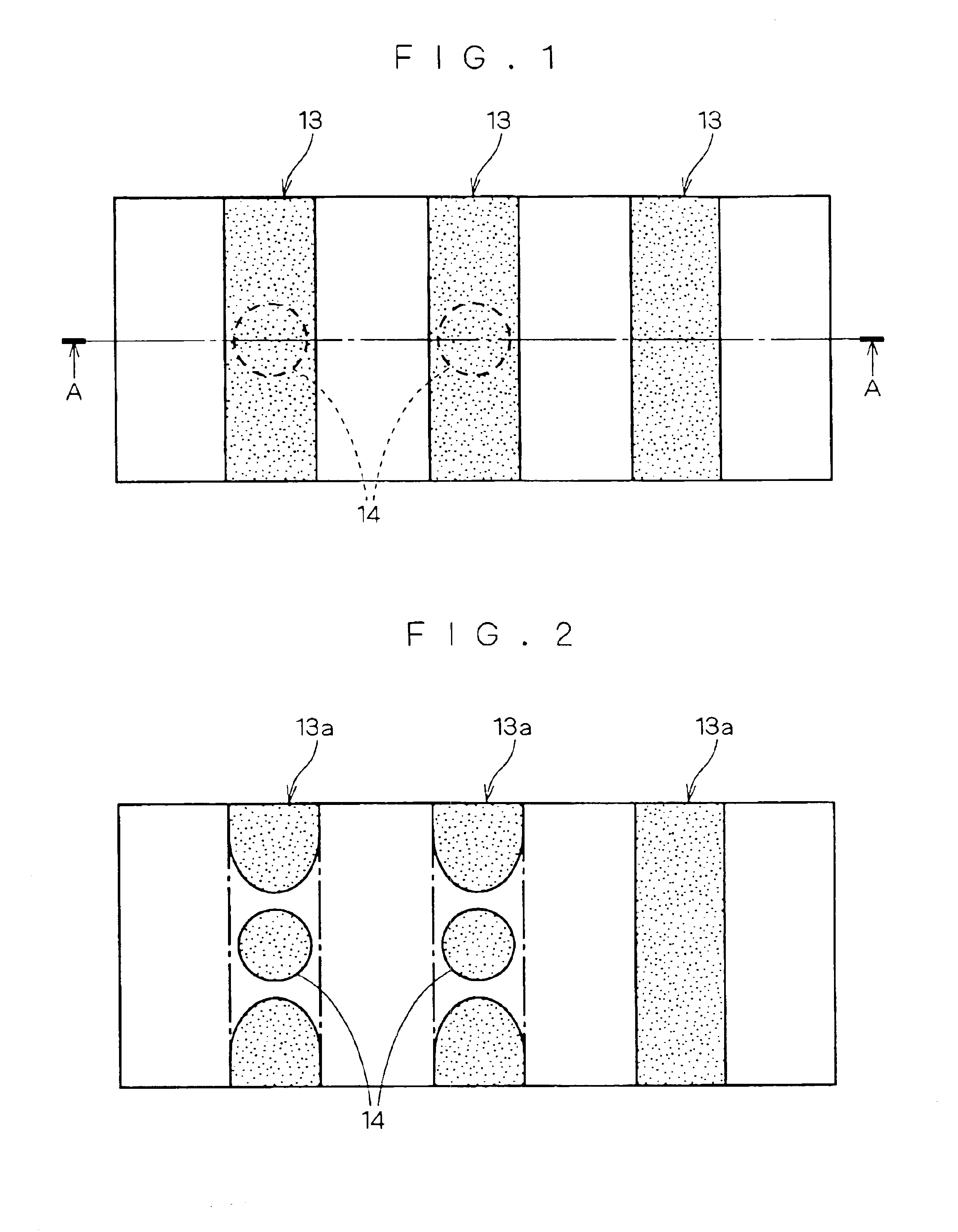
first embodiment
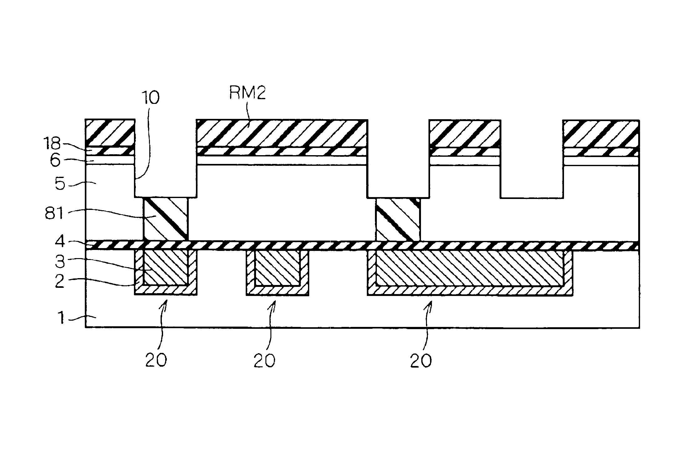
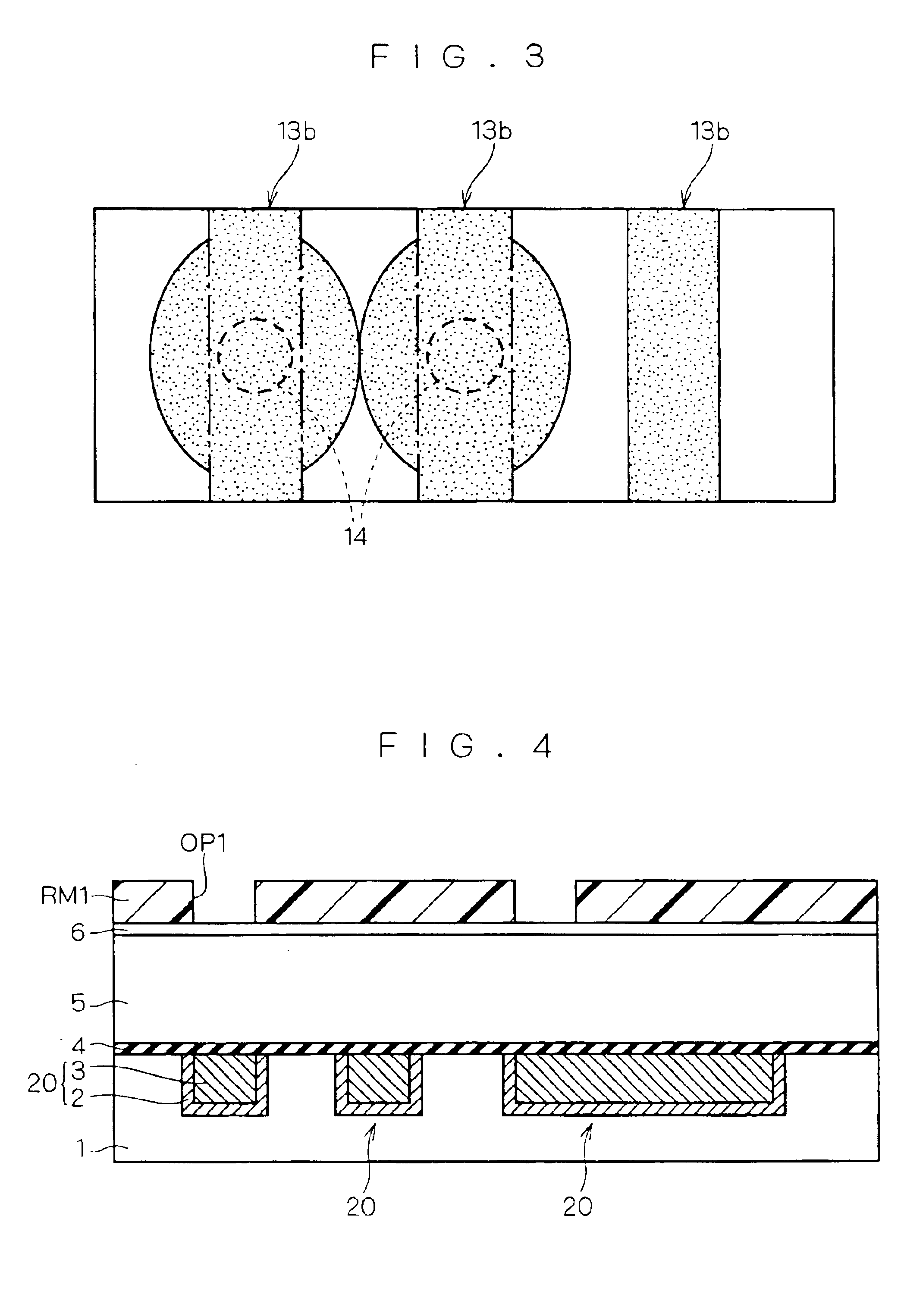
[0032]As the present invention, a method of manufacturing a semiconductor device 100 having a multilayer wiring structure will be described below with reference to FIGS. 4 to 14 to be sectional views showing a manufacturing process in order. A structure of the semiconductor device 100 is shown in FIG. 14 illustrating a final step. Moreover, the sectional views of FIGS. 4 to 14 correspond to sectional views taken along an A—A portion in FIG. 1.
[0033]
[0034]First of all, at a step shown in FIG. 4, a lower wiring 20 is formed by a general damascene method in a main surface of an underlying layer (for example, a silicon substrate) 1. The lower wiring 20 is formed by covering an internal wall of a trench formed in the main surface of the underlying layer 1 with a barrier metal layer 2 and burying a metal wiring layer 3 formed of copper or the like in a region surrounded by the barrier metal layer 2. The underlying layer 1 is not restricted to a silicon substrate but an interlayer dielectr...
second embodiment
[0086]As the present invention, a method of manufacturing a semiconductor device 200 having a multilayer wiring structure will be described below with reference to FIGS. 20 to 29 to be sectional views showing a manufacturing process in order. A structure of the semiconductor device 200 is shown in FIG. 29 illustrating a final step. Moreover, the same structures as those in FIGS. 1 to 14 have the same reference numerals and repetitive description will be omitted.
[0087]
[0088]At a step shown in FIG. 20, first of all, an interlayer dielectric film 51 having a low dielectric constant including a siloxane bonding in a main structure is provided in a thickness of 200 to 1000 nm on an etching stopper film 4 of an insulator, for example. A material such as a carbon-doped SiO film formed by a CVD method, methylsilsesquioxane (MSQ) formed by a coating method or the like is used for the interlayer dielectric film 51 having a low dielectric constant.
[0089]Then, an etching stopper film 41 having ...
PUM
| Property | Measurement | Unit |
|---|---|---|
| Temperature | aaaaa | aaaaa |
| Temperature | aaaaa | aaaaa |
| Time | aaaaa | aaaaa |
Abstract
Description
Claims
Application Information