Nitride semiconductor light-emitting device

a technology of semiconductor light-emitting device and nitride, which is applied in the direction of semiconductor devices, electrical devices, nanotechnology, etc., can solve the problems of device to realize a strong band-to-band emission, laser oscillation is not possible, and the half band width of the emission spectrum cannot avoid widening. achieve excellent laser oscillation

Inactive Publication Date: 2005-05-31
NICHIA CORP
View PDF37 Cites 33 Cited by
  • Summary
  • Abstract
  • Description
  • Claims
  • Application Information

AI Technical Summary

Benefits of technology

[0011]Therefore, a first object of the present invention is to provide a nitride semiconductor light-emitting device which is capable of generating an excellent laser oscillation.
[0012]A second object of the present invention is to provide a nitride semiconductor light-emitting device which is capable of exhibiting an improved emission output.
[0046]According to the present invention, there is further provided a nitride semiconductor light-emitting device comprising an active layer comprising a nitride semiconductor containing at least indium and interposed between a first n-type clad layer comprising an n-type nitride semiconductor having a smaller thermal expansion coefficient than that of the active layer and a first p-type clad layer comprising a p-type nitride semiconductor having a smaller thermal expansion coefficient than that of the active layer, wherein the active layer is of a single-quantum well structure or of a multi-quantum well structure, thereby to emit a light of lower energy than the inherent band gap energy of the nitride semiconductor forming the active layer.
[0047]According to the present invention, there is further provided a nitride semiconductor light-emitting device comprising a first n-type clad layer made of an n-type nitride semiconductor containing indium or of an n-type GaN; and an active layer comprising a nitride semiconductor containing indium, having a larger thermal expansion coefficient than that of the first n-type clad layer and provided in contact with the first n-type clad layer, wherein the active layer is of a single-quantum well structure or of a multi-quantum well structure, thereby to emit a light of lower energy than the inherent band gap energy of the nitride semiconductor forming the active layer.

Problems solved by technology

However, since an InGaN layer doped with impurities is utilized as an active layer in this LED device, this LED device is accompanied with a drawback that the half band width of emission spectrum can not avoid from becoming wide.
As for LD device, it is theoretically possible to realize a laser oscillation in a double-heterostructure comprising an active layer formed of a non-doped InGaN as described in the above-mentioned Unexamined Japanese Patent Application Publication 6-21511, but the laser oscillation is not yet realized with such a double-heterostructure.
However, there are many problems to be solved, such as the preparation of an optical resonance surface or of an optical confinement layer, before the LD device can be actually realized.
However, the thickness of the active layer in the conventional LED device is relatively thick, i.e., 0.1 to 0.2 μm, thus the thickness of InGaN layer hetero-epitaxially grown on an AlGaN layer already exceeds over the critical thickness, so that it was impossible with the conventional LED device to realize a strong band-to-band emission, thus failing to realize a laser oscillation.
However, if the thickness of the active layer is thinned, the light confinement may then become insufficient thus making it impossible to realize a laser oscillation.

Method used


Image

  • Nitride semiconductor light-emitting device
  • Nitride semiconductor light-emitting device
  • Nitride semiconductor light-emitting device

Examples


example 1

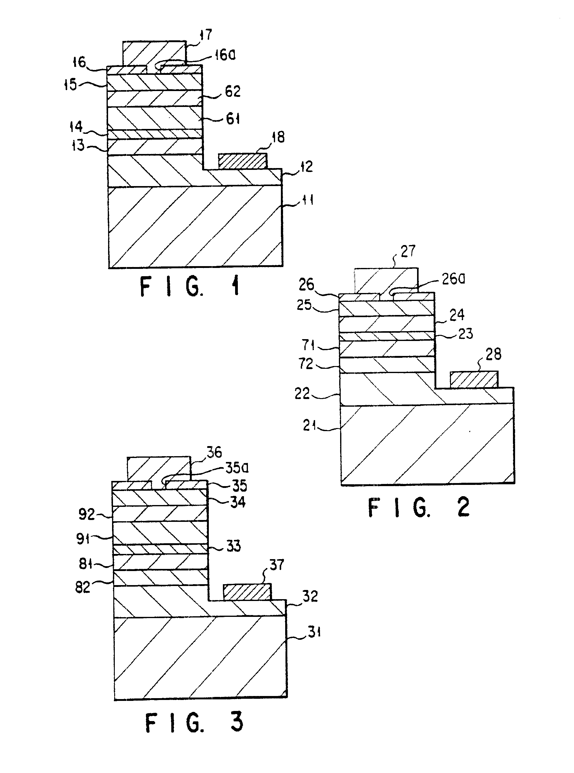
[0177]This Example 1 will be explained with reference to FIG. 1 as follows.

[0178]First, using TMG (trimethylgallium) and NH3 as raw materials, a buffer layer formed of GaN was grown at a temperature of 500° C. to a thickness of 200 angstroms on the C-plane of a sapphire substrate 11 which had been set in advance in a reaction vessel.

[0179]Then, the temperature was raised up to 1050° C., upon which silane gas was added to the TMG and NH3, thereby growing an n-type contact layer 12 consisting of Si-doped n-type GaN to a thickness of 4 μm in thickness.

[0180]Subsequently, the temperature was lowered down to 800° C., and TMI (trimethylindium) was added to the raw material gas thereby growing an n-type clad layer 13 formed of Si-doped n-type In0.05Ga0.95N to a thickness of 500 angstroms.

[0181]While keeping this temperature of 800° C., an active layer 14 of a single-quantum well structure consisting of non-doped n-type In0.2Ga0.8N was grown to a thickness of 20 angstroms.

[0182]Then, the te...

example 2

[0187]This Example 2 will be explained with reference to FIG. 2 as follows.

[0188]In the same manner as in Example 1, a GaN buffer layer having a thickness of 200 angstroms was formed on a sapphire substrate 21, and an n-type contact layer 22 consisting of n-type GaN was formed to a thickness of 4 μm by the MOVPE method.

[0189]Then, after forming a second n-type clad layer 72 having a thickness of 0.5 μm and formed of Si-doped n-type Al0.3Ga0.7N, a first n-type clad layer 71 having a thickness of 500 angstroms and consisting of Si-doped n-type In0.05Ga0.95N was formed.

[0190]Then, an active layer 23 of a single-quantum well structure having a thickness of 20 angstroms and consisting of non-doped In0.2Ga0.8N was grown, and then a p-type clad layer 24 having a thickness of 0.5 μm and consisting of a Mg-doped p-type Al0.3Ga0.7N, and a p-type contact layer 25 having a thickness of 1.0 μm in thickness and consisting of Mg-doped GaN were successively deposited thereover.

[0191]Then, the same ...

example 3

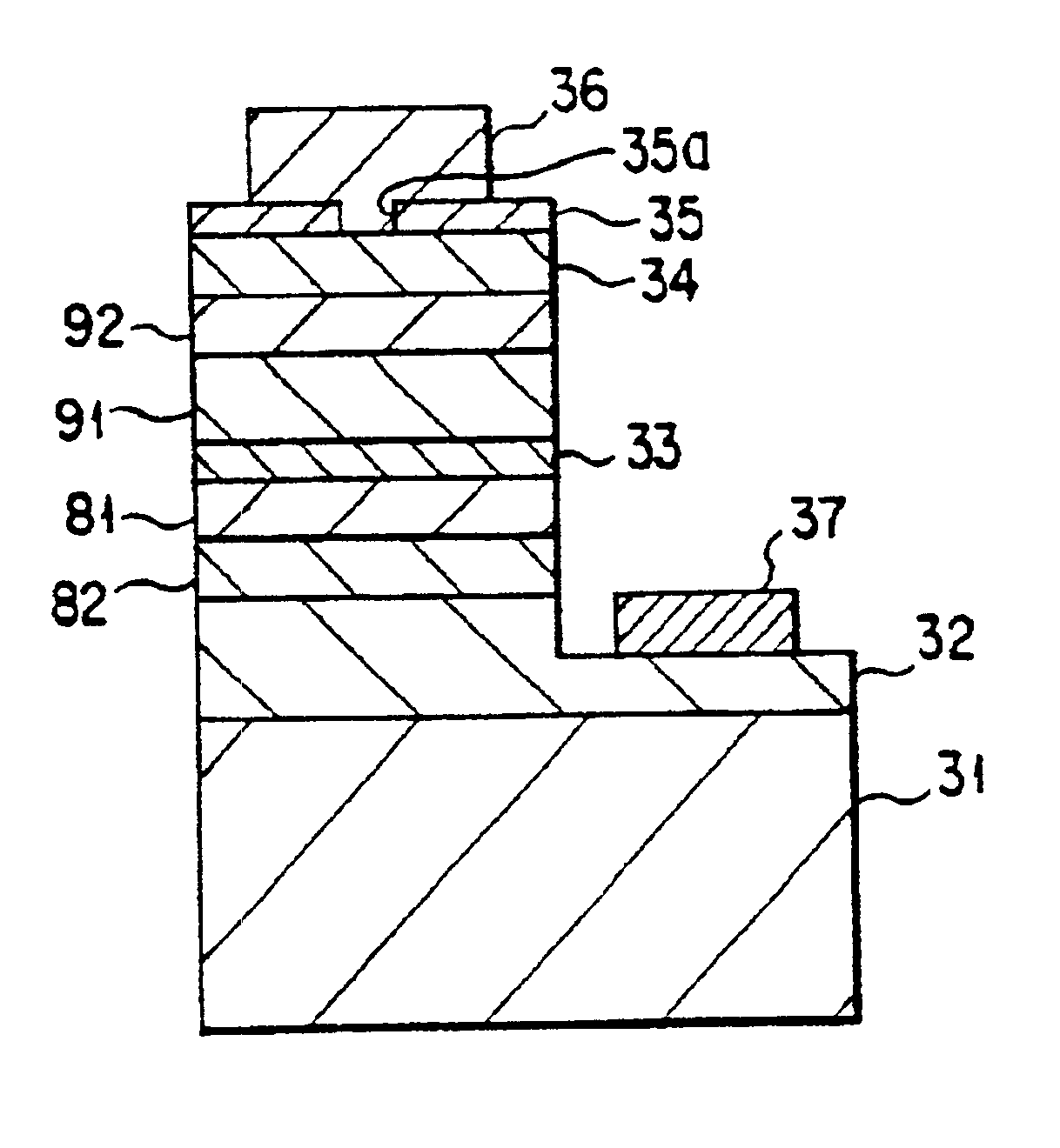
[0192]This Example 3 will be explained with reference to FIG. 3 as follows.

[0193]First, a GaN buffer layer having a thickness of 200 angstroms, and an n-type contact layer 32 having a thickness of 4 μm and consisting of n-type GaN were formed in the same manner as in Example 1 on a sapphire substrate 31 by the MOVPE method.

[0194]Then, after forming a second n-type clad layer 82 having a thickness of 0.5 μm and formed of Si-doped n-type Al0.3Ga0.7N, a first n-type clad layer 81 having a thickness of 0.1 μm and consisting of Si-doped n-type In0.05Ga0.95N was formed.

[0195]Then, an active layer 23 of a single-quantum well structure having a thickness of 20 angstroms and consisting of non-doped In0.2Ga0.8N was grown, and then a first p-type clad layer 91 having a thickness of 0.1 μm and consisting of a Mg-doped p-type Al0.3Ga0.7N, a second p-type clad layer 92 having a thickness of 0.5 μm and consisting of a Mg-doped p-type Al0.3Ga0.7N, and a p-type contact layer 34 having a thickness of...


PUM

PropertyMeasurementUnit
emission wavelengthaaaaaaaaaa
thicknessaaaaaaaaaa
thicknessaaaaaaaaaa

Abstract

A nitride semiconductor light-emitting device has an active layer of a single-quantum well structure or multi-quantum well made of a nitride semiconductor containing indium and gallium. A first p-type clad layer made of a p-type nitride semiconductor containing aluminum and gallium is provided in contact with one surface of the active layer. A second p-type clad layer made of a p-type nitride semiconductor containing aluminum and gallium is provided on the first p-type clad layer. The second p-type clad layer has a larger band gap than that of the first p-type clad layer. An n-type semiconductor layer is provided in contact with the other surface of the active layer.

Description

[0001]This application is a continuation of application Ser. No. 09 / 069,240, filed Apr. 29, 1998, now abandoned, the entire content of which is hereby incorporated by reference in this application, now abandoned.BACKGROUND OF THE INVENTION[0002]1. Field of the Invention[0003]The present invention relates to a semiconductor light-emitting device such as a light-emitting diode (LED) or a laser diode (LD), and in particular to a light-emitting device having a semiconductor structure formed of all nitride semiconductor materials.[0004]2. Description of the Related Art[0005]As materials for a light-emitting device such as an LED or LD device which is expected of emitting a light ranging from ultraviolet to red, nitride semiconductor materials (InxAlyGa1−x−yN; 0≦x, 0≦y, x+y≦1) are known, and blue and blue-green LEDs have been put to practical use in, for example, displays or signals.[0006]The light-emitting device such as a blue LED or a blue-green LED formed of nitride semiconductor mate...

Claims


Application Information

Patent Timeline
Patent Type & Authority Patents(United States)
IPC IPC(8): H01L33/00H01L33/06H01L33/32
CPCB82Y20/00H01L33/32H01L33/06
Inventor NAKAMURA, SHUJINAGAHAMA, SHINICHIIWASA, NARUHITOKIYOKU, HIROYUKI
Owner NICHIA CORP
Why Eureka
Try Eureka